
Projected

About the Projected PCB
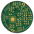
Projected is an open source STM32 PCB design by jonnor, published on GitHub. It is a 2-layer board measuring 28 × 28 mm, with 43 components from 26 distinct parts.
Its main chip is the STM32L432KBU6, from the STM32 family. Other key parts include the MCP73812T-420I-OT, PCA9306DCUR, MCP1640BT-I/CHY, TPS7A0533PDBVT and LIS2DE12TR. By type, the board carries 16 resistors, 11 capacitors, 7 ICs, 5 connectors, 1 transistor and 1 battery holder.
It belongs with the robotics & motion and power & battery designs in this gallery.
From the project
Small projects not worthy of dedicated repositories
Etsy.com. Lots of amazing looking products. Mostly rings,pendants. Pure resin or resin+wood. 200-400 NOK. Sometimes glow-in-the-dark. Resin 'stone' with wood base, silver ring inlay. 700-800 NOK.
Maybe silver + resin cast rings has good opportunity? Not found, might be able to push price up.
Oxididation. Electroetching with laser-engraved masks?
Power board for wearable or other battery powered electronics.
Main components on the Projected
Projected bill of materials (BOM)
43 components, 26 distinct parts.
| Qty | Part | Footprint | Refs |
|---|---|---|---|
| 1 | STM32L432KBU6 | QFN-32-1EP_5x5mm_P0.5mm_EP3.45x3.45mm | U1 |
| 1 | MCP73812T-420I-OT | SOT-23-5 | U2 |
| 1 | PCA9306DCUR | VSSOP-8_2.3x2mm_P0.5mm | U3 |
| 1 | MCP1640BT-I/CHY | SOT-23-6 | U4 |
| 1 | TPS7A0533PDBVT | SOT-23-5 | U5 |
| 1 | LIS2DE12TR | LGA-12_2x2mm_P0.5mm | U6 |
| 1 | MIC | XDCR_CMM-4030DT-26154-TR | U7 |
| 1 | BC847CL | SOT-23 | Q1 |
| 1 | TOUCH | Pins_1x04_P1.27mm | J1 |
| 1 | DOCK | Pins_1x06_P1.27mm | J3 |
| 1 | Leds | Pins_1x04_P1.27mm | J4 |
| 1 | SWD | Pins_1x06_P1.27mm | J5 |
| 1 | EXT | Pins_1x06_P1.27mm | J6 |
| 1 | LIR2450 | LIR2450-horizontal-pins | BT1 |
| 1 | LED | LED_0603_1608Metric_Pad1.05x0.95mm_HandSolder | D2 |
| 1 | 4.7uH | L_0805_2012Metric_Pad1.15x1.40mm_HandSolder | L1 |
| 1 | C | C_0603_1608Metric_Pad1.05x0.95mm_HandSolder | C1 |
| 10 | 1uF | C_0603_1608Metric_Pad1.05x0.95mm_HandSolder | C2, C3, C4, C5, C6, C7, C8, C9 +2 |
| 2 | 1k | R_0603_1608Metric_Pad1.05x0.95mm_HandSolder | R1, R2 |
| 3 | R | R_0603_1608Metric_Pad1.05x0.95mm_HandSolder | R3, R8, R9 |
Show 6 more
| Qty | Part | Footprint | Refs |
|---|---|---|---|
| 1 | 22k | R_0603_1608Metric_Pad1.05x0.95mm_HandSolder | R4 |
| 2 | 10k | R_0603_1608Metric_Pad1.05x0.95mm_HandSolder | R5, R6 |
| 2 | 4k7 | R_0603_1608Metric_Pad1.05x0.95mm_HandSolder | R7, R12 |
| 1 | 330k | R_0603_1608Metric_Pad1.05x0.95mm_HandSolder | R10 |
| 3 | 100k | R_0603_1608Metric_Pad1.05x0.95mm_HandSolder | R11, R13, R14 |
| 2 | 3k3 | R_0603_1608Metric_Pad1.05x0.95mm_HandSolder | R15, R16 |
Projected design files
The KiCad project lives in the jonnor/projects repository on GitHub; these links point at the commit this page was built from.
Projected: common questions
What microcontroller does the Projected use?
The Projected is built around the STM32L432KBU6, from the STM32 family.
How big is the Projected PCB?
The Projected measures 28 × 28 mm, has 2 copper layers and is 1.6 mm thick.
How many components are on the Projected?
43 components, from 26 distinct parts. The full bill of materials is listed on this page.
Where can I download the Projected design files?
From the jonnor/projects repository on GitHub, which has the KiCad layout; the links under Design files point to each one.
Can I use the Projected design in my own project?
The repository has no license, so all rights stay with jonnor. Use it as a reference, and ask the author before reusing the design.
Can I test firmware for the Projected without the hardware?
Yes. HardLabs builds a simulation of the board from its netlist and BOM, so you can run and debug STM32 firmware against it before you order a PCB.
More boards in projects
Digishaper152
80 × 60 mm60 parts2LNo license43
Toggle
48.5 × 67.7 mm24 parts2LNo license43
Touchled
23.6 × 23.6 mm18 parts2LNo license43
Linearsource mod
45.7 × 22.2 mm17 parts2LNo license43 AVR/Arduino
Touchuc
13 × 13 mm16 parts2LNo license43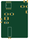
Crystaltriggeramp
25 × 34 mm11 parts2LNo license43
Pendantlight
5 × 40 mm10 parts2LNo license43
Ledbreakout
10 × 10 mm9 parts2LNo license43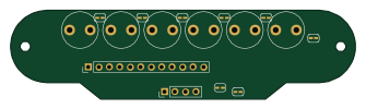
Scpu10
83.6 × 21.5 mm8 parts2LNo license43
Touchflower
10.6 × 10.6 mm7 parts2LNo license43
Similar boards
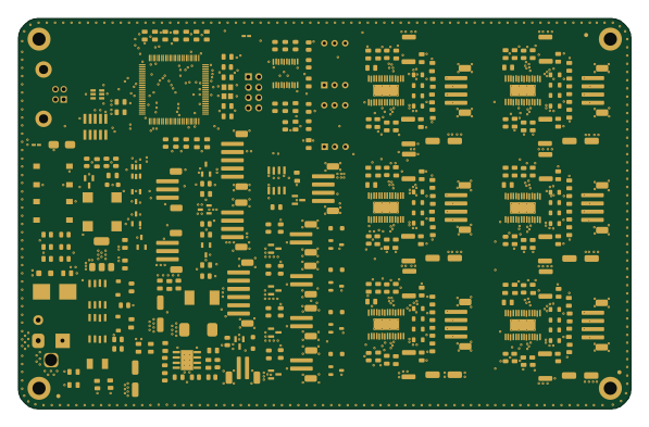 STM32
STM32LumenPnP Motherboard
opulo-inc
149 × 95 mm296 parts4LCC-BY-SA-4.03.7k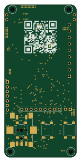 STM32
STM32AxxSolder
AxxAxx
39 × 82.5 mm122 parts2LGPL-3.01.7k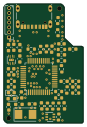 STM32
STM32AIOC
skuep
21 × 31.5 mm47 parts2LMIT1.4k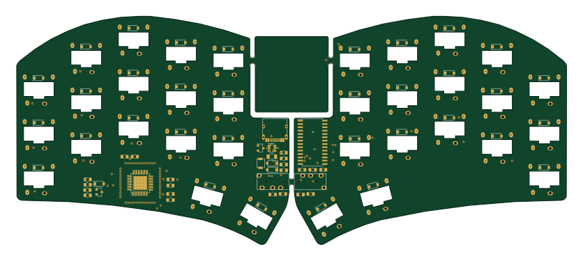 STM32
STM32Ferris
pierrechevalier83
208.8 × 86.8 mm102 parts2LSHL-2.11.3k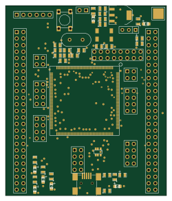 STM32
STM32176 pin board
rusefi
61.8 × 73.2 mm76 parts2LGPL-3.01.2k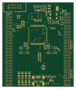 STM32
STM32Brain board STM32F407
61.8 × 73.2 mm69 parts2LGPL-3.01.2k