
Kcell faker

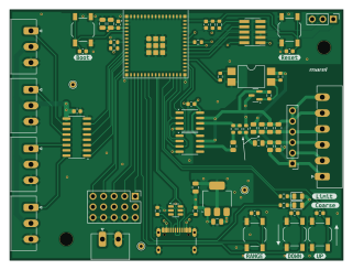
About the Kcell faker PCB
Kcell faker is an open source ESP32 PCB design by karlp, published on GitHub. It is a 4-layer board measuring 80 × 60 mm, with 62 components from 35 distinct parts.
Its main chip is the ESP32-S3-MINI-1-N8, from the ESP32 family. Other key parts include the MCP4131-104E/SN, AMS1117-33, SRV05-4, ULN2003ADR and EL817S1(C)(TU)-F. By type, the board carries 23 resistors, 13 capacitors, 10 connectors, 7 ICs, 5 switches and 2 diodes.
It belongs with the iot & wireless designs in this gallery.
From the project
fake a load cell, for testing functional behaviour with changing loads.
fake a load cell, for testing functional behaviour with changing loads.
this is NOT intended for use with calibration or accuracy testing, but to help simulate response to changing loads
USB (or wifi/bt....) control of a bridge differential....
Main components on the Kcell faker
Kcell faker bill of materials (BOM)
62 components, 35 distinct parts — part numbers from the project's BOM.
| Qty | Part | Footprint | Refs |
|---|---|---|---|
| 2 | MCP4131-104E/SN | SOIC-8_3.9x4.9mm_P1.27mm | U1, U4 |
| 1 | AMS1117-33 | SOT-223-3_TabPin2 | U2 |
| 1 | SRV05-4 | SOT-23-6 | U3 |
| 1 | ULN2003ADR ULN2003A | SOIC-16_3.9x9.9mm_P1.27mm | U5 |
| 1 | ESP32-S3-MINI-1-N8 ESP32-S3-MINI-1 | ESP32-S2-MINI-1 | U6 |
| 1 | EL817S1(C)(TU)-F LTV-817S | SMDIP-4_W9.53mm | U7 |
| 1 | HX PZ2.54-3x5P ZZ Servo_x5 | PinHeader_3x05_P2.54mm_Vertical | M7 |
| 1 | AO3400A | SOT-23 | Q1 |
| 1 | JL15EDGRC-38106G01 Conn_01x06 | PhoenixContact_MC_1,5_6-G-3.81_1x06_P3.81mm_Horizontal | J1 |
| 1 | DB2ERC-3.81-2P-BK Conn_01x02 | PhoenixContact_MC_1,5_2-G-3.81_1x02_P3.81mm_Horizontal | J2 |
| 1 | HB-PH9-12725PB2GOB Conn_ARM_JTAG_SWD_10 | PinHeader_2x05_P1.27mm_Vertical_SMD | J3 |
| 1 | C2937625 DBG | PinHeader_1x03_P2.54mm_Vertical | J4 |
| 1 | Conn_01x06 | PinHeader_1x06_P2.54mm_Vertical | J5 |
| 1 | USB-TYPE-C-018 USB_C_Receptacle_USB2.0_16P | USB_C_Receptacle_GCT_USB4105-xx-A_16P_TopMnt_Horizontal | J6 |
| 4 | WJ15EDGRC-3.81-3P Conn_01x03 | PhoenixContact_MC_1,5_3-G-3.81_1x03_P3.81mm_Horizontal | J7, J8, J9, J10 |
| 1 | TS-1187A-B-A-B BOOT | SW_SPST_TL3342 | SW1 |
| 1 | TS-1187A-B-A-B RST | SW_SPST_TL3342 | SW2 |
| 1 | TS-1187A-B-A-B UP | SW_SPST_TL3342 | SW3 |
| 1 | TS-1187A-B-A-B DOWN | SW_SPST_TL3342 | SW4 |
| 1 | TS-1187A-B-A-B RANGE | SW_SPST_TL3342 | SW5 |
Show 15 more
| Qty | Part | Footprint | Refs |
|---|---|---|---|
| 1 | NCD0805R1 red | LED_0805_2012Metric | D1 |
| 1 | KT-0805G green | LED_0805_2012Metric | D3 |
| 4 | CL21A106KAYNNNE 10uF | C_0805_2012Metric | C1, C3, C4, C5 |
| 8 | CC0603KRX7R9BB104 100nF | C_0603_1608Metric | C2, C6, C7, C8, C10, C11, C12, C14 |
| 1 | CL10A105KB8NNNC 1uF | C_0603_1608Metric | C9 |
| 4 | 0603WAF3300T5E 330 | R_0603_1608Metric | R1, R12, R13, R18 |
| 4 | 0805W8F3300T5E 330 | R_0805_2012Metric | R2, R3, R4, R23 |
| 2 | 0805W8F3302T5E 33k | R_0805_2012Metric | R5, R14 |
| 1 | 0805W8F2203T5E 220k | R_0805_2012Metric | R6 |
| 2 | 0603WAF5101T5E 5k1 | R_0603_1608Metric | R7, R8 |
| 3 | 0603WAF1002T5E 10k | R_0603_1608Metric | R9, R20, R22 |
| 4 | 0603WAF0000T5E 0R | R_0603_1608Metric | R10, R11, R16, R17 |
| 1 | 0805W8F1503T5E 150k | R_0805_2012Metric | R15 |
| 1 | 0603WAF5100T5E 510R | R_0603_1608Metric | R19 |
| 1 | 0603WAF3302T5E 33k | R_0603_1608Metric | R21 |
Kcell faker design files
The KiCad project lives in the karlp/kcell-faker repository on GitHub; these links point at the commit this page was built from.
Kcell faker: common questions
What microcontroller does the Kcell faker use?
The Kcell faker is built around the ESP32-S3-MINI-1-N8, from the ESP32 family.
How big is the Kcell faker PCB?
The Kcell faker measures 80 × 60 mm, has 4 copper layers and is 1.626 mm thick.
How many components are on the Kcell faker?
62 components, from 35 distinct parts, with part numbers taken from the project's own BOM. The full bill of materials is listed on this page.
Where can I download the Kcell faker design files?
From the karlp/kcell-faker repository on GitHub, which has the KiCad layout, the schematic and the BOM; the links under Design files point to each one.
Can I use the Kcell faker design in my own project?
The repository has no license, so all rights stay with karlp. Use it as a reference, and ask the author before reusing the design.
Can I test firmware for the Kcell faker without the hardware?
Yes. HardLabs builds a simulation of the board from its netlist and BOM, so you can run and debug ESP32 firmware against it before you order a PCB.
Similar boards
 ESP32
OSO-BOOK-B1
joeycastillo
85 × 115 mm65 parts2LCC-BY-SA-4.08.1k ESP32
Powertrain
byrantech
64 × 45.4 mm171 parts4LMIT4.3k ESP32
Esp32 minimal
atopile
36.2 × 26.8 mm20 parts2LMIT4.0k ESP32
Badge
56.3 × 39 mm239 parts4LMIT4.0k ESP32
Racer
StuckAtPrototype
36 × 50.2 mm70 parts4LApache-2.03.8k ESP32
Controller
29 × 74 mm58 parts4LApache-2.03.8k