
Mbed ce ci shield v2

About the Mbed ce ci shield v2
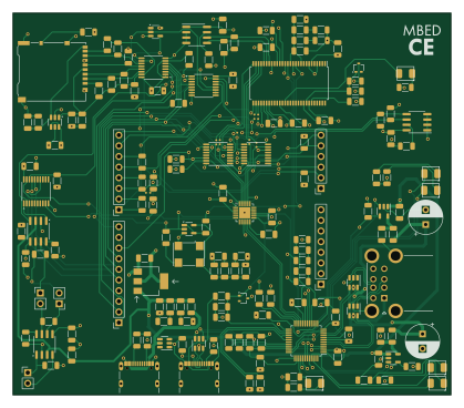
Mbed ce ci shield v2 is an open source PCB design by mbed-ce, published on GitHub under the CERN-OHL-P-2.0 license. It is a 4-layer board measuring 104.5 × 91 mm, with 164 components from 49 distinct parts.
Other key parts include the CY7C68013A-56PVX, CY7C65632-48AXCT, USBLC6-2SC6, BD2221G-LBTR and LD1117S33TR. By type, the board carries 64 resistors, 51 capacitors, 22 ICs, 11 connectors, 8 diodes and 7 inductors.
It belongs with the test & measurement, dev boards & breakouts and usb & debug tools designs in this gallery.
From the project
New version of the Mbed OS CE CI Shield -- a shield containing a logic analyzer and components to test features like I2C, SPI, and PWM.
Note: I swear I'm not sponsored by Infineon or anything, it just so happened that their chips were the best fit for everything I needed on the board. I even tried to use an FT232H in the first rev of the hardware, but I could not for the life of me get it to work.
It can test up to 10 different types of IO: | IO Type | Test Method | |---|---| | USB Device | The Mbed target's USB Device port can be connected to one of the shield's downstream USB ports | | SPI Master | The Mbed target can interact with the MicroSD card. The logic analyzer can observe this interaction. | | SPI Slave | The…

Main components on the Mbed ce ci shield v2
Mbed ce ci shield v2 bill of materials (BOM)
164 components, 49 distinct parts — part numbers from the project's BOM.
| Qty | Part | Footprint | Refs |
|---|---|---|---|
| 1 | CY7C68013A-56PVX | SSOP-56_7.5x18.5mm_P0.635mm | U1 |
| 1 | CY7C65632-48AXCT | LQFP-48_7x7mm_P0.5mm | U2 |
| 4 | USBLC6-2SC6 | SOT-23-6 | U3, U4, U5, U8 |
| 2 | BD2221G-LBTR | SOT-23-5 | U6, U7 |
| 1 | LD1117S33TR | SOT-223-3_TabPin2 | U9 |
| 1 | CY7C65211A | QFN-24-1EP_4x4mm_P0.5mm_EP2.65x2.65mm-LengthenedPads | U10 |
| 2 | SN74CB3Q3253PWR | TSSOP-16_4.4x5mm_P0.65mm | U11, U12 |
| 1 | ADG733BRU | TSSOP-16_4.4x5mm_P0.65mm | U13 |
| 1 | 74AHC1G04 | SOT-23-5 | U14 |
| 2 | 24FC64-I/SN | SOIC-8_3.9x4.9mm_P1.27mm | U15, U16 |
| 1 | MCP2515-XST MCP2515-xST | TSSOP-20_4.4x6.5mm_P0.65mm | U17 |
| 2 | TJA1051T-3 | SOIC-8_3.9x4.9mm_P1.27mm | U18, U19 |
| 1 | 74LVC1G80 | SOT-23-5 | U20 |
| 1 | SN74AXC4T774 | TSSOP-16_4.4x5mm_P0.65mm | U21 |
| 1 | AP22913W6-7 | SOT-23-6 | U22 |
| 1 | 24.000MHZ 24.000MHz | Oscillator_SMD_Abracon_ASV-4Pin_7.0x5.1mm | X1 |
| 2 | USB4105-GF-A | USB_C_Receptacle_GCT_USB4105-xx-A_16P_TopMnt_Horizontal-ExtraHoleClearance | J1, J3 |
| 1 | UJ2-ADH-3-TH | USB_A_CUI_UJ2-ADH-TH_Horizontal_Stacked | J2 |
| 2 | 1X8 1x8 | PinSocket_1x08_P2.54mm_Vertical | J4, J5 |
| 1 | 1X6 1x6 | PinSocket_1x06_P2.54mm_Vertical | J6 |
Show 29 more
| Qty | Part | Footprint | Refs |
|---|---|---|---|
| 1 | 1X10 1x10 | PinSocket_1x10_P2.54mm_Vertical | J7 |
| 1 | DM3AT | microSD_HC_Hirose_DM3AT-SF-PEJM5 | J8 |
| 3 | 1X2 1x2 | PinHeader_1x02_P2.54mm_Vertical | J9, J10, J11 |
| 2 | AA3528CGSK | AA3528 | D1, D2 |
| 2 | AA3528SYSK | AA3528 | D3, D4 |
| 2 | AA3528SURSK | AA3528 | D5, D6 |
| 2 | BAT54W | SOT-323_SC-70 | D7, D8 |
| 7 | 732-4654-1 300@100MHz | R_1206_3216Metric | FB1, FB2, FB3, FB4, FB5, FB6, FB7 |
| 23 | 100NF 100nF | C_1206_3216Metric | C1, C3, C4, C6, C7, C10, C11, C16 +15 |
| 11 | 2.2UF 2.2uF | C_1206_3216Metric | C2, C5, C8, C9, C12, C13, C19, C21 +3 |
| 12 | 1u | C_1206_3216Metric | C14, C15, C22, C25, C26, C28, C29, C30 +4 |
| 3 | 10U 10u | C_1206_3216Metric | C17, C37, C43 |
| 2 | 100U 100u | CP_Radial_D8.0mm_P3.50mm | C18, C20 |
| 1 | 649 | R_1206_3216Metric | R1 |
| 4 | 5.1K 5.1k | R_1206_3216Metric | R2, R3, R11, R12 |
| 9 | 100K 100k | R_1206_3216Metric | R4, R5, R6, R7, R8, R9, R10, R16 +1 |
| 1 | 9.1K 9.1k | R_1206_3216Metric | R13 |
| 2 | 4.7K 4.7k | R_1206_3216Metric | R14, R25 |
| 20 | 10K 10k | R_1206_3216Metric | R15, R22, R23, R24, R26, R31, R35, R36 +12 |
| 2 | 270 | R_1206_3216Metric | R17, R18 |
| 3 | 300 | R_1206_3216Metric | R19, R20, R21 |
| 4 | 1k | R_1206_3216Metric | R27, R28, R30, R62 |
| 1 | 1.5K 1.5k | R_1206_3216Metric | R29 |
| 2 | 120 | R_1206_3216Metric | R32, R44 |
| 2 | 1.1K 1.1k | R_1206_3216Metric | R33, R34 |
| 2 | 2.2K 2.2k | R_1206_3216Metric | R37, R38 |
| 1 | 820 | R_1206_3216Metric | R41 |
| 8 | 1 | R_1206_3216Metric | R46, R47, R48, R49, R50, R51, R54, R55 |
| 2 | 33 | R_1206_3216Metric | R52, R53 |
Mbed ce ci shield v2 design files
The KiCad project lives in the mbed-ce/mbed-ce-ci-shield-v2 repository on GitHub; these links point at the commit this page was built from.
Mbed ce ci shield v2: common questions
How big is the Mbed ce ci shield v2?
The Mbed ce ci shield v2 measures 104.5 × 91 mm, has 4 copper layers and is 1.58 mm thick.
How many components are on the Mbed ce ci shield v2?
164 components, from 49 distinct parts, with part numbers taken from the project's own BOM. The full bill of materials is listed on this page.
Where can I download the Mbed ce ci shield v2 design files?
From the mbed-ce/mbed-ce-ci-shield-v2 repository on GitHub, which has the KiCad layout, the schematic and the BOM; the links under Design files point to each one.
Can I use the Mbed ce ci shield v2 design in my own project?
Yes, under the terms of its CERN-OHL-P-2.0 license, which mbed-ce chose for the repository.
Similar boards
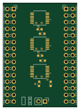
LevelShifter
gusmanb
28.3 × 39.8 mm21 parts2LGPL-3.05.0k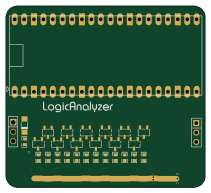
AnalyzerBoxPCB fork
52.7 × 47.9 mm54 parts4LGPL-3.05.0k
StackLink
52.3 × 10.5 mm5 parts2LGPL-3.05.0k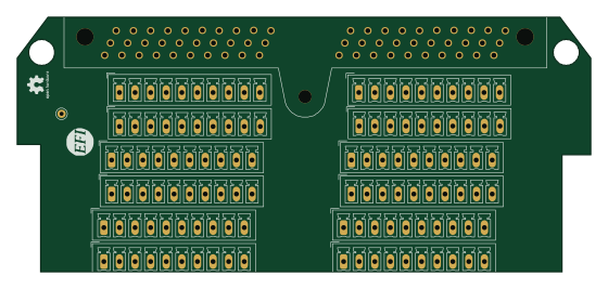
Breakout 60pin EEC-IV
rusefi
139.7 × 62.2 mm15 parts2LGPL-3.01.2k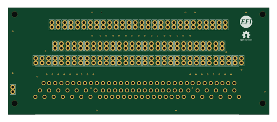
88 Pin Vag Breakout
142 × 58 mm91 parts2LGPL-3.01.2k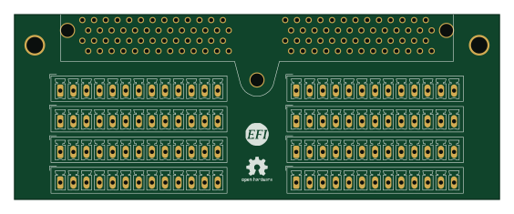
Eecv breakout
140.8 × 53.7 mm9 parts4LGPL-3.01.2k