
VibePCB-LA

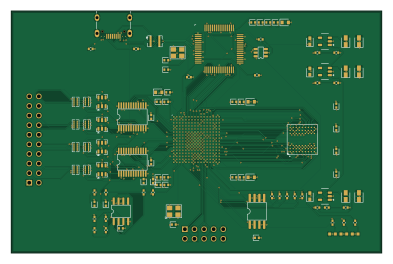
About the VibePCB-LA PCB
VibePCB-LA is an open source FPGA PCB design by PaulBichl, published on GitHub. It is a 6-layer board measuring 98 × 64 mm, with 103 components from 34 distinct parts.
Its main chip is the LFE5U-25F-7BG256I, from the FPGA family. Other key parts include the IS42S16160J-7BLI, FT2232HL-REEL, USBLC6-2SC6, 93LC56BT-I/OT and SN74LVC8T245PWR. By type, the board carries 40 capacitors, 36 resistors, 12 ICs, 7 diodes, 3 connectors and 3 inductors.
From the project
A 16-channel, 100 MSa/s USB 2.0 HS logic analyzer: a Lattice ECP5 FPGA (CABGA-256 BGA) capturing into a 32 MB SDRAM (54-ball BGA), read out over an FT2232H. 98 x 64 mm, 6 layers. Designed with VibePCB (tscircuit -> KiCad) as a stretch of the tooling: two 0.8 mm BGAs escaped and r
A 16-channel, 100 MSa/s USB 2.0 HS logic analyzer: a Lattice ECP5 FPGA (CABGA-256 BGA) capturing into a 32 MB SDRAM (54-ball BGA), read out over an FT2232H. 98 x 64 mm, 6 layers. Designed with VibePCB (tscircuit -> KiCad) as a stretch of the tooling: two 0.8 mm BGAs escaped and routed by VibePCB's own router, a length-checked 39-signal memory bus, a coupled 90 ohm USB pair, three power planes.
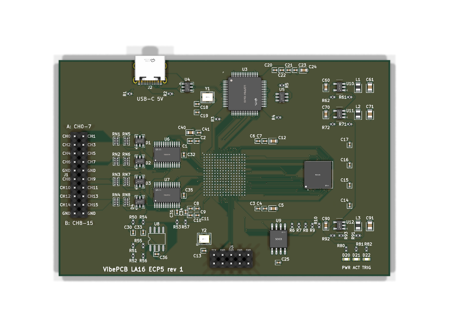
Main components on the VibePCB-LA
VibePCB-LA bill of materials (BOM)
103 components, 34 distinct parts — part numbers from the project's BOM.
| Qty | Part | Footprint | Refs |
|---|---|---|---|
| 1 | LFE5U-25F-7BG256I | LFE5U-25F-7BG256I | U1 |
| 1 | IS42S16160J-7BLI | IS42S16160J-7BLI | U2 |
| 1 | FT2232HL-REEL | FT2232HL-REEL | U3 |
| 1 | USBLC6-2SC6 | USBLC6-2SC6 | U4 |
| 1 | 93LC56BT-I/OT | 93LC56BT-I_OT | U5 |
| 2 | SN74LVC8T245PWR | SN74LVC8T245PWR | U6, U7 |
| 1 | TLV9062IDR | TLV9062IDR | U8 |
| 1 | W25Q128JVSIQ | W25Q128JVSIQ | U9 |
| 3 | TLV62569DBVR | TLV62569DBVR | U10, U11, U12 |
| 1 | X322512MSB4SI | X322512MSB4SI | Y1 |
| 1 | SX3M100.000B20F30TNN | SX3M100_000B20F30TNN | Y2 |
| 1 | PIN_HEADER_PINROW20_P2_54_NOPINLABELS_ROWS2 pin_header_pinrow20_p2_54_nopinlabels_rows2 | pin_header_pinrow20_p2_54_nopinlabels_rows2 | J1 |
| 1 | TYPE-C-31-M-12 | TYPE-C-31-M-12 | J2 |
| 1 | PIN_HEADER_PINROW10_P2_54_ROWS2 pin_header_pinrow10_p2_54_rows2 | pin_header_pinrow10_p2_54_rows2 | J5 |
| 4 | SRV05-4 | SRV05-4 | D1, D2, D3, D4 |
| 3 | KT-0603G | KT-0603G | D20, D21, D22 |
| 3 | C63167 2.2µH | inductor_0805 | L1, L2, L3 |
| 24 | 100NF 100nF | capacitor_cap0402 | C1, C2, C3, C4, C6, C7, C8, C9 +16 |
| 6 | 10UF 10uF | capacitor_cap0603 | C5, C12, C40, C60, C70, C90 |
| 2 | 18PF 18pF | capacitor_cap0402 | C18, C19 |
Show 14 more
| Qty | Part | Footprint | Refs |
|---|---|---|---|
| 1 | 4.7UF 4.7uF | capacitor_cap0603 | C24 |
| 4 | 1UF 1uF | capacitor_cap0402 | C30, C31, C33, C34 |
| 3 | 22UF 22uF | capacitor_cap0805 | C61, C71, C91 |
| 2 | 5.1kΩ | resistor_res0402 | R1, R2 |
| 2 | 12kΩ | resistor_res0402 | R3, R71 |
| 13 | 10kΩ | resistor_res0402 | R4, R6, R7, R8, R9, R10, R50, R51 +5 |
| 1 | 2.2kΩ | resistor_res0402 | R5 |
| 2 | 20kΩ | resistor_res0402 | R52, R56 |
| 2 | 10Ω | resistor_res0402 | R53, R57 |
| 2 | 22kΩ | resistor_res0402 | R61, R92 |
| 1 | 100kΩ | resistor_res0402 | R62 |
| 3 | 330Ω | resistor_res0402 | R80, R81, R82 |
| 4 | 4D02WGJ0102TCE | 4D02WGJ0102TCE | RN1, RN2, RN3, RN4 |
| 4 | RTA02-4D105JTH | RTA02-4D105JTH | RN5, RN6, RN7, RN8 |
VibePCB-LA design files
The KiCad project lives in the PaulBichl/VibePCB-LA repository on GitHub; these links point at the commit this page was built from.
VibePCB-LA: common questions
What microcontroller does the VibePCB-LA use?
The VibePCB-LA is built around the LFE5U-25F-7BG256I, from the FPGA family.
How big is the VibePCB-LA PCB?
The VibePCB-LA measures 98 × 64 mm, has 6 copper layers and is 1.6 mm thick.
How many components are on the VibePCB-LA?
103 components, from 34 distinct parts, with part numbers taken from the project's own BOM. The full bill of materials is listed on this page.
Where can I download the VibePCB-LA design files?
From the PaulBichl/VibePCB-LA repository on GitHub, which has the KiCad layout, the schematic and the BOM; the links under Design files point to each one.
Can I use the VibePCB-LA design in my own project?
The repository has no license, so all rights stay with PaulBichl. Use it as a reference, and ask the author before reusing the design.
Can I test firmware for the VibePCB-LA without the hardware?
Yes. HardLabs builds a simulation of the board from its netlist and BOM, so you can run and debug FPGA firmware against it before you order a PCB.
Similar boards
 FPGA
Base board
GlasgowEmbedded
80 × 49 mm222 parts4L0BSD2.2k FPGA
Thunderscope Rev5.3
EEVengers
122.5 × 103.5 mm817 parts6LMIT1.3k FPGA
Usb sniffer
ataradov
58.2 × 38.1 mm86 parts2LBSD-3-Clause1.3k FPGA
Tomu, I'm
theacodes
13 × 9.4 mm40 parts4LMIT1.1k FPGA
Icepi zero
cheyao
65 × 30 mm143 parts4LSHL-2.1865 FPGA
Gcvideo
ikorb
49 × 30 mm44 parts4LNo license765