
EPS

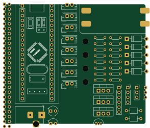
About the EPS PCB
EPS is an open source PCB design by Amr-H25, published on GitHub. It is a 2-layer board measuring 73.3 × 62.1 mm, with 45 components from 27 distinct parts.
Other key parts include the LM35-LP, YAAJ_BluePill, L7805 and LD1117S33TR_SOT223. By type, the board carries 16 resistors, 10 connectors, 7 ICs, 5 diodes, 4 capacitors and 3 transistors.
It belongs with the science & space designs in this gallery.
From the project
A simulated CubeSat for Earth observation: captures images and transmits them to a ground station for processing and analysis. Final-year graduation project at Helwan University.
Main components on the EPS
EPS bill of materials (BOM)
45 components, 27 distinct parts.
| Qty | Part | Footprint | Refs |
|---|---|---|---|
| 1 | LM35-LP | TO-92_Inline | U1 |
| 1 | YAAJ_BluePill | YAAJ_BluePill_1 | U2 |
| 1 | ~ | PinSocket_1x06_P2.54mm_Vertical | U3 |
| 1 | ~ | PinSocket_1x04_P2.54mm_Vertical | U4 |
| 1 | L7805 | PinSocket_1x03_P2.54mm_Vertical | U5 |
| 1 | LD1117S33TR_SOT223 | PinSocket_1x03_P2.54mm_Vertical | U6 |
| 1 | ~ | MT3608 Module | U7 |
| 3 | IRF540N | TO-220-3_Vertical | Q1, Q2, Q3 |
| 1 | GPIO | PinHeader_2x26_P2.54mm_Vertical | J1 |
| 1 | +X | JST_EH_B2B-EH-A_1x02_P2.50mm_Vertical | J2 |
| 1 | -X | JST_EH_B2B-EH-A_1x02_P2.50mm_Vertical | J3 |
| 1 | +Y | JST_EH_B2B-EH-A_1x02_P2.50mm_Vertical | J4 |
| 1 | -Y | JST_EH_B2B-EH-A_1x02_P2.50mm_Vertical | J5 |
| 1 | Battery Connector 3.7 | JST_EH_B2B-EH-A_1x02_P2.50mm_Vertical | J6 |
| 1 | Solar Out | JST_EH_B2B-EH-A_1x02_P2.50mm_Vertical | J7 |
| 1 | Bat Out | JST_EH_B2B-EH-A_1x02_P2.50mm_Vertical | J8 |
| 1 | Barrel_Jack_Switch | BarrelJack_Horizontal | J9 |
| 1 | UART_DEBUG | JST_EH_B2B-EH-A_1x02_P2.50mm_Vertical | J10 |
| 5 | 1N5817 | D_DO-41_SOD81_P10.16mm_Horizontal | D1, D2, D3, D4, D5 |
| 1 | 100nF | C_Axial_L3.8mm_D2.6mm_P7.50mm_Horizontal | C1 |
Show 7 more
| Qty | Part | Footprint | Refs |
|---|---|---|---|
| 1 | 0.1uF | CP_Radial_Tantal_D5.0mm_P2.50mm | C2 |
| 1 | 0.33uF | C_Axial_L3.8mm_D2.6mm_P7.50mm_Horizontal | C3 |
| 1 | 10uF | CP_Radial_Tantal_D5.0mm_P2.50mm | C4 |
| 5 | 10K | R_Axial_DIN0204_L3.6mm_D1.6mm_P5.08mm_Horizontal | R1, R3, R5, R15, R16 |
| 3 | 220 | R_Axial_DIN0204_L3.6mm_D1.6mm_P5.08mm_Horizontal | R2, R4, R6 |
| 4 | 47K | R_Axial_DIN0204_L3.6mm_D1.6mm_P5.08mm_Horizontal | R7, R8, R9, R10 |
| 4 | 33K | R_Axial_DIN0204_L3.6mm_D1.6mm_P5.08mm_Horizontal | R11, R12, R13, R14 |
EPS design files
The KiCad project lives in the Amr-H25/CubeSat-EarthObservation repository on GitHub; these links point at the commit this page was built from.
EPS: common questions
How big is the EPS PCB?
The EPS measures 73.3 × 62.1 mm, has 2 copper layers and is 1.6 mm thick.
How many components are on the EPS?
45 components, from 27 distinct parts. The full bill of materials is listed on this page.
Where can I download the EPS design files?
From the Amr-H25/CubeSat-EarthObservation repository on GitHub, which has the KiCad layout and the schematic; the links under Design files point to each one.
Can I use the EPS design in my own project?
The repository has no license, so all rights stay with Amr-H25. Use it as a reference, and ask the author before reusing the design.
More boards in CubeSat-EarthObservation
Similar boards
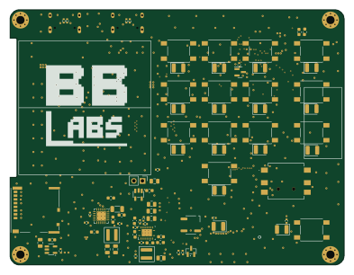
PiFinder4
brickbots
98 × 75 mm150 parts4LGPL-3.0250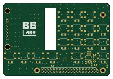
PiFinder smt
93.8 × 64.2 mm47 parts2LGPL-3.0250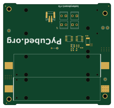
Batteryboard
pycubed
95.9 × 90.2 mm28 parts2LNo license97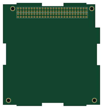
CubeSatKit StackBoard
imciner2
90.2 × 95.9 mm3 partsCC-BY-SA-4.065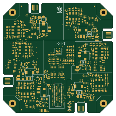
Fox-1-MPPT
FaradayRF
95 × 95 mm453 parts4LCustom license62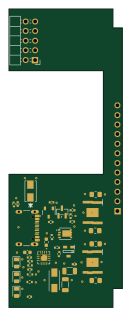
Usbc power
SoukeyCircuits
30 × 79 mm41 parts2LGPL-3.055