
Fmc usb gpio spi jtag

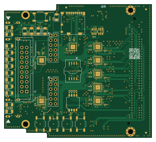
About the Fmc usb gpio spi jtag PCB
Fmc usb gpio spi jtag is an open source PCB design by chipsalliance, published on GitHub under the Apache-2.0 license. It is a 6-layer board measuring 76.5 × 69 mm, with 136 components from 36 distinct parts.
Other key parts include the M24C02-FMN, STUSB03EQR, CH9102F, TXS02612RTWR and AIP74LVC1T45GB236TR. By type, the board carries 54 resistors, 31 capacitors, 19 ICs, 17 diodes, 8 connectors and 6 switches.
It belongs with the usb & debug tools designs in this gallery.
From the project
PCB libraries and templates for rocket-chip based FPGA/ASIC designs
The basic peripherals of the FPGA mezzanine card, including JTAG, UART, GPIO, USB, I3C, etc., can be used for prototype verification of the basic peripherals of the SoC.
When using it for the first time, it is necessary to program the IPMI FRU data for the EEPROM so that the development board can identify the power supply of the FMC.
If you only need to build the eeprom binary,
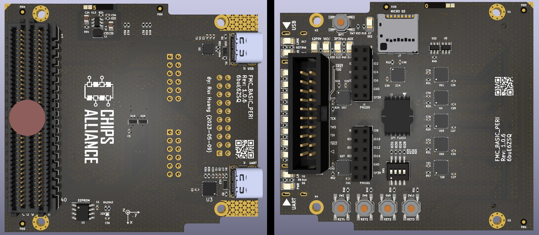
Main components on the Fmc usb gpio spi jtag
Fmc usb gpio spi jtag bill of materials (BOM)
136 components, 36 distinct parts.
| Qty | Part | Footprint | Refs |
|---|---|---|---|
| 1 | M24C02-FMN | SOIC-8_3.9x4.9mm_P1.27mm | U1 |
| 1 | STUSB03EQR | QFN_B03EQR_STM | U2 |
| 1 | CH9102F | QFN-24-1EP_4x4mm_P0.5mm_EP2.6x2.6mm | U3 |
| 8 | TXS02612RTWR | WQFN-24-1EP_4x4mm_P0.5mm_EP2.45x2.45mm | U4, U11, U14, U15, U16, U17, U26, U27 |
| 2 | AIP74LVC1T45GB236TR | SOT-23-6 | U5, U22 |
| 4 | TPD4E02B04DQA | USON-10_2.5x1.0mm_P0.5mm | U12, U18, U19, U20 |
| 1 | MT2492 | SOT-23-6 | U13 |
| 1 | MMC5603NJ | WLP4_N40P2X2_80X80X52N | U25 |
| 1 | SAMTEC_ASP-134604-01 | Samtec_FMC_ASP-134604-01_4x40_P1.27mm | J1 |
| 1 | ACA-SPI-004-K02 | ACA-SPI-004 | J2 |
| 2 | USB_C_Receptacle | USB_C_Receptacle_Molex_105450-0101 | J3, J4 |
| 1 | Conn_JTAG_20 | IDC-Header_2x10_P2.54mm_Vertical | J5 |
| 2 | PM2.54-2x6 | PinSocket_2x06_P2.54mm_Vertical_PMOD | J6, J8 |
| 1 | Micro_SD_Card_Det2 | microSD_HC_Molex_104031-0811 | J7 |
| 1 | DSHP04TSGET | SW_DIP_SPSTx04_Slide_KingTek_DSHP04TS_W7.62mm_P1.27mm | SW1 |
| 5 | TL3342F160QG | SW_SPST_TL3342 | SW2, SW7, SW8, SW9, SW10 |
| 11 | NCD1206Y1 | LED_1206_3216Metric | D1, D2, D3, D4, D5, D7, D8, D9 +3 |
| 6 | NCD1206O1 | LED_1206_3216Metric | D6, D12, D13, D14, D15, D16 |
| 1 | 4.7uH ±20% 1.6A TFM252012ALMA4R7MTAA | L_Sunlord_SWPA252012S | L1 |
| 21 | 100n | C_0402_1005Metric | C1, C2, C5, C7, C8, C22, C23, C25 +13 |
Show 16 more
| Qty | Part | Footprint | Refs |
|---|---|---|---|
| 2 | 1u | C_0402_1005Metric | C3, C10 |
| 3 | 4.7u | C_0402_1005Metric | C4, C6, C9 |
| 1 | 22u ±20% 35V | C_0805_2012Metric | C24 |
| 1 | 22n | C_0402_1005Metric | C33 |
| 1 | 22p | C_0402_1005Metric | C34 |
| 1 | 22u | C_0805_2012Metric | C35 |
| 1 | 0.1u | C_0402_1005Metric | C36 |
| 5 | 5.1k | R_0402_1005Metric | R1, R2, R3, R4, R35 |
| 16 | 6.8k | R_0402_1005Metric | R5, R6, R7, R8, R9, R10, R18, R29 +8 |
| 20 | 10k | R_0402_1005Metric | R11, R12, R19, R20, R21, R22, R25, R26 +12 |
| 7 | 47k | R_0402_1005Metric | R13, R14, R15, R16, R17, R23, R24 |
| 1 | 100k 1% | R_0402_1005Metric | R33 |
| 1 | 22k 1% | R_0402_1005Metric | R34 |
| 1 | 0R(DNI) | R_0402_1005Metric | R36 |
| 2 | 20R | R_0402_1005Metric | R44, R53 |
| 1 | 15k | R_0402_1005Metric | R54 |
Fmc usb gpio spi jtag design files
The KiCad project lives in the chipsalliance/rocket-pcb repository on GitHub; these links point at the commit this page was built from.
Fmc usb gpio spi jtag: common questions
How big is the Fmc usb gpio spi jtag PCB?
The Fmc usb gpio spi jtag measures 76.5 × 69 mm, has 6 copper layers and is 1.617 mm thick.
How many components are on the Fmc usb gpio spi jtag?
136 components, from 36 distinct parts. The full bill of materials is listed on this page.
Where can I download the Fmc usb gpio spi jtag design files?
From the chipsalliance/rocket-pcb repository on GitHub, which has the KiCad layout and the schematic; the links under Design files point to each one.
Can I use the Fmc usb gpio spi jtag design in my own project?
Yes, under the terms of its Apache-2.0 license, which chipsalliance chose for the repository.
More boards in rocket-pcb
Similar boards
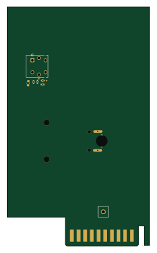
XG Station Power
osy
54.3 × 91 mm9 parts2LCC-BY-4.0703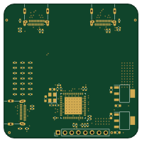
USB Hub Test
50 × 50 mm85 parts4LCC-BY-4.0703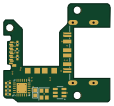
FW-EC-DongleHiderPlus
LeoDJ
28.2 × 26.1 mm14 parts4LCERN-OHL-W-2.0490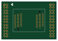
Adapter tsop48
bbogush
48 × 33 mm3 parts2LGPL-3.0389
Adapter tsop48 solder
48 × 33 mm3 parts2LGPL-3.0389
Adapter soic8 solder
48 × 20 mm3 parts2LGPL-3.0389