
Device


About the Device PCB
Device is an open source STM32 PCB design by jayis1, published on GitHub. It is a 4-layer board measuring 85 × 54 mm, with 21 components from 19 distinct parts.
Its main chip is the STM32H743VIT6, from the STM32 family. Other key parts include the iCE40UP5K-SG48I, MT41K256M16TW-107:P, USB3320C-EZK, TPS6521815RSLR and BQ25896RTWR. By type, the board carries 10 ICs, 4 switches, 3 crystals, 2 connectors and 2 LEDs.
It belongs with the power & battery and displays & leds designs in this gallery.
From the project
Full-cycle hardware designs for security research devices — each device is a subfolder with its own README, schematics, PCB layout, and software stack
A portable, self-contained hardware platform for direct, hardware-level extraction of raw flash memory from embedded devices, IoT endpoints, smartphones, automotive ECUs, and industrial controllers.
The eMMC Flash Dumper connects directly to flash memory ICs — eMMC, raw NAND, or SPI NOR — and performs a bit-for-bit readout at the electrical level. This makes it immune to OS-level anti-forensics, locked bootloaders, and filesystem encryption that operates above the block layer.
Main components on the Device
Device bill of materials (BOM)
21 components, 19 distinct parts.
| Qty | Part | Footprint | Refs |
|---|---|---|---|
| 1 | STM32H743VIT6 | LQFP-100_14x14mm_P0.5mm | U1 |
| 1 | iCE40UP5K-SG48I | QFN-48-1EP_7x7mm_P0.5mm | U2 |
| 1 | MT41K256M16TW-107:P | FBGA-96_9x14mm_P0.8mm | U3 |
| 1 | USB3320C-EZK | QFN-32-1EP_5x5mm_P0.5mm | U4 |
| 1 | TPS6521815RSLR | VQFN-48-1EP_7x7mm_P0.5mm | U5 |
| 1 | BQ25896RTWR | WQFN-24-1EP_4x4mm_P0.5mm | U6 |
| 2 | TXS0108EPWR | TSSOP-20_4.4x6.5mm_P0.65mm | U7, U8 |
| 1 | SSD1306 OLED | SSD1306_0.96inch_128x64 | U10 |
| 1 | TPS74801DRCR | VSON-10-1EP_3x3mm_P0.5mm | U11 |
| 1 | 25MHz | Crystal_SMD_Abracon_ABM8G-4Pin_3.2x2.5mm | Y1 |
| 1 | 32.768kHz | Crystal_SMD_Abracon_ABS07-2Pin_3.2x1.5mm | Y2 |
| 1 | 12MHz | Crystal_SMD_Abracon_ABM8G-4Pin_3.2x2.5mm | Y3 |
| 1 | USB4105-GF-A | USB_C_Receptacle_GCT_USB4105 | J1 |
| 1 | ISP Header | PinHeader_2x10_P2.54mm_Vertical | J3 |
| 1 | UP | SW_SPST_PTS645 | SW1 |
| 1 | DOWN | SW_SPST_PTS645 | SW2 |
| 1 | SELECT | SW_SPST_PTS645 | SW3 |
| 1 | BACK | SW_SPST_PTS645 | SW4 |
| 2 | WS2812B | LED_WS2812B-Mini | LED1, LED2 |
Device design files
The KiCad project lives in the jayis1/hacker-devices repository on GitHub; these links point at the commit this page was built from.
Device: common questions
What microcontroller does the Device use?
The Device is built around the STM32H743VIT6, from the STM32 family.
How big is the Device PCB?
The Device measures 85 × 54 mm, has 4 copper layers and is 1.6 mm thick.
How many components are on the Device?
21 components, from 19 distinct parts. The full bill of materials is listed on this page.
Where can I download the Device design files?
From the jayis1/hacker-devices repository on GitHub, which has the KiCad layout and the schematic; the links under Design files point to each one.
Can I use the Device design in my own project?
The repository has no license, so all rights stay with jayis1. Use it as a reference, and ask the author before reusing the design.
Can I test firmware for the Device without the hardware?
Yes. HardLabs builds a simulation of the board from its netlist and BOM, so you can run and debug STM32 firmware against it before you order a PCB.
More boards in hacker-devices
- schematic only · 48 partsSTM32
Silent symphony
48 partsNo license3  ESP32
ESP32Chronos phantom
65 × 30 mm26 parts4LNo license3 STM32
STM32Trace reaper
85.5 × 24 mm24 parts4LNo license3 ESP32
ESP32Spectre-Sniffer
80 × 320 mm23 parts4LNo license3 STM32
STM32ACOUSTIC-PHANTOM — Acoustic Side-Channel Analyzer
120 × 22 mm20 parts4LNo license3 STM32
STM32GHOSTBUS — Covert SWD/JTAG Hardware Debug Implant
50 × 24 mm18 parts4LNo license3 RP2040/RP2350
FiberPhantom — Covert Fiber Optic Network Tap & MITM Implant
82 × 34 mm17 parts4LNo license3
Joule-Phantom — Smart-Battery SMBus MITM Implant
90 × 70 mm14 parts4LNo license3 STM32
STM32Forge-Probe: Silicon Backdoor Debug Probe
37 × 23 mm11 parts4LNo license3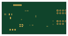 STM32
STM32TPM-PHANTOM — Trusted Platform Module Bus Analyzer
60 × 30 mm9 parts4LNo license3 STM32
STM32AxleTap — Automotive Ethernet Tap
120 × 125 mm8 parts4LNo license3
Similar boards
 STM32
STM32LumenPnP Motherboard
opulo-inc
149 × 95 mm296 parts4LCC-BY-SA-4.03.7k STM32
STM32AxxSolder
AxxAxx
39 × 82.5 mm122 parts2LGPL-3.01.7k STM32
STM32LibreVNA
jankae
122 × 98 mm592 parts6LGPL-3.01.6k STM32
STM32AIOC
skuep
21 × 31.5 mm47 parts2LMIT1.4k STM32
STM32Ferris
pierrechevalier83
208.8 × 86.8 mm102 parts2LSHL-2.11.3k STM32
STM32176 pin board
rusefi
61.8 × 73.2 mm76 parts2LGPL-3.01.2k