
TWIN NODE2

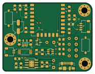
About the TWIN NODE2 PCB
TWIN NODE2 is an open source ESP8266 PCB design by MAATHES-THILAK-K, published on GitHub under the Apache-2.0 license. It is a 2-layer board measuring 46.6 × 35.5 mm, with 41 components from 24 distinct parts.
Its main chip is the ESP-12F, from the ESP8266 family. Other key parts include the RT9080-33GJ5, TP4056-42-ESOP8 and DW01A. By type, the board carries 15 resistors, 9 capacitors, 5 diodes, 4 ICs, 4 connectors and 2 transistors.
It belongs with the iot & wireless, power & battery and sensors designs in this gallery.
From the project
ESP-NOW based solar-powered water level monitoring system for overhead tanks. An outdoor ESP8266 node uses a waterproof ultrasonic sensor to measure water level and transmits data wirelessly without internet. Designed for ultra-low power, outdoor reliability, and real-world deployment.
The Indoor Node is a battery-powered, ultra-low-power receiver and alert unit for the TWIN-NODE water level monitoring system. It receives water level data from the outdoor sensor node using ESP-NOW and provides local LED and buzzer alerts, without internet or Wi-Fi infrastructure.
ESP-NOW wireless communication Battery-powered operation Ultra-low-power design LED level indication Buzzer alert for critical levels No internet, no router, no cloud
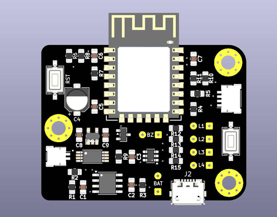
Main components on the TWIN NODE2
TWIN NODE2 bill of materials (BOM)
41 components, 24 distinct parts.
| Qty | Part | Footprint | Refs |
|---|---|---|---|
| 1 | RT9080-33GJ5 | SOT94P280X100-5N | IC1 |
| 1 | ESP-12F | ESP-12F | U1 |
| 1 | TP4056-42-ESOP8 | SOIC-8-1EP_3.9x4.9mm_P1.27mm_EP2.41x3.3mm_ThermalVias | U2 |
| 1 | DW01A | SOT-23-6 | U3 |
| 1 | FS8205A | SOP65P640X120-8N | Q1 |
| 1 | BSS138 | SOT-23 | Q2 |
| 1 | 01x02 | SolderWire-0.1sqmm_1x02_P3.6mm_D0.4mm_OD1mm | J1 |
| 1 | USB_B_Micro | USB_Micro-B_Molex_47346-0001 | J2 |
| 1 | 01x02 | JST_SH_SM02B-SRSS-TB_1x02-1MP_P1.00mm_Horizontal | J3 |
| 1 | 01x04 | JST_SH_SM04B-SRSS-TB_1x04-1MP_P1.00mm_Horizontal | J4 |
| 1 | RST | SW_Tactile_SPST_NO_Straight_CK_PTS636Sx25SMTRLFS | SW1 |
| 1 | BOOT | SW_Tactile_SPST_NO_Straight_CK_PTS636Sx25SMTRLFS | SW2 |
| 1 | LED_BLUE | SolderWire-0.1sqmm_1x02_P3.6mm_D0.4mm_OD1mm | D1 |
| 4 | LED | SolderWire-0.1sqmm_1x02_P3.6mm_D0.4mm_OD1mm | D2, D3, D4, D5 |
| 5 | 10uF | C_0805_2012Metric_Pad1.18x1.45mm_HandSolder | C1, C2, C5, C8, C9 |
| 1 | 0.1uF | C_0805_2012Metric_Pad1.18x1.45mm_HandSolder | C3 |
| 1 | 100uF | CP_Elec_5x5.3 | C4 |
| 2 | 100nF | C_0805_2012Metric_Pad1.18x1.45mm_HandSolder | C6, C7 |
| 2 | 1k | R_0805_2012Metric_Pad1.20x1.40mm_HandSolder | R1, R9 |
| 1 | 2k | R_0805_2012Metric_Pad1.20x1.40mm_HandSolder | R2 |
Show 4 more
| Qty | Part | Footprint | Refs |
|---|---|---|---|
| 1 | 100 | R_0805_2012Metric_Pad1.20x1.40mm_HandSolder | R3 |
| 5 | 12k | R_0805_2012Metric_Pad1.20x1.40mm_HandSolder | R4, R5, R7, R8, R10 |
| 2 | 10k | R_0805_2012Metric_Pad1.20x1.40mm_HandSolder | R6, R11 |
| 4 | 330 | R_0805_2012Metric_Pad1.20x1.40mm_HandSolder | R12, R13, R14, R15 |
TWIN NODE2 design files
The KiCad project lives in the MAATHES-THILAK-K/TWIN-NODE repository on GitHub; these links point at the commit this page was built from.
TWIN NODE2: common questions
What microcontroller does the TWIN NODE2 use?
The TWIN NODE2 is built around the ESP-12F, from the ESP8266 family.
How big is the TWIN NODE2 PCB?
The TWIN NODE2 measures 46.6 × 35.5 mm, has 2 copper layers and is 1.6 mm thick.
How many components are on the TWIN NODE2?
41 components, from 24 distinct parts. The full bill of materials is listed on this page.
Where can I download the TWIN NODE2 design files?
From the MAATHES-THILAK-K/TWIN-NODE repository on GitHub, which has the KiCad layout and the schematic; the links under Design files point to each one.
Can I use the TWIN NODE2 design in my own project?
Yes, under the terms of its Apache-2.0 license, which MAATHES-THILAK-K chose for the repository.
Can I test firmware for the TWIN NODE2 without the hardware?
Yes. HardLabs builds a simulation of the board from its netlist and BOM, so you can run and debug ESP8266 firmware against it before you order a PCB.
More boards in TWIN-NODE
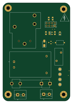
Similar boards
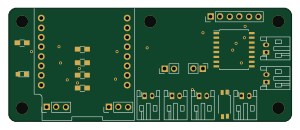 ESP8266
ESP8266ControllerCircuit
stuartpittaway
75 × 30 mm20 parts2LCC-BY-NC-4.01.1k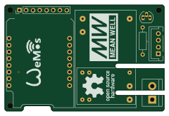 ESP8266
HASwitchPlate
aderusha
60 × 40 mm8 parts2LMIT738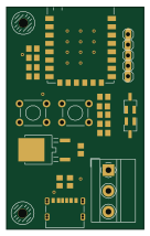 ESP8266
Goatgdo
Kaldek
32.9 × 53.3 mm23 parts2LMIT506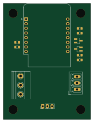 ESP8266
RatGDO-OpenSource-D1Mini-ESP8266
47.8 × 63.3 mm12 parts2LMIT506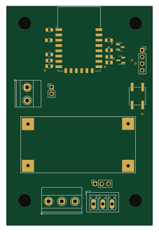 ESP8266
RatGDO-OpenSource-Bare-ESP8266
55 × 82.7 mm20 parts2LMIT506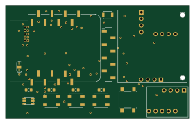 ESP8266
Iaq board
nkitanov
70.1 × 43.2 mm17 parts2LNo license398