
Smartpowerbank2026

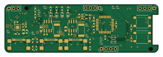
About the Smartpowerbank2026 PCB
Smartpowerbank2026 is an open source ESP8266 PCB design by MAIK97MAX, published on GitHub. It is a 4-layer board measuring 83 × 26 mm, with 71 components from 32 distinct parts.
Its main chip is the ESP-12E, from the ESP8266 family. Other key parts include the ATMEGA328-A, AP2112K-3.3, INA219AXD, BQ27441-G1 and BQ24074RGT. By type, the board carries 27 resistors, 22 capacitors, 8 ICs, 3 connectors, 2 switches and 2 LEDs.
It belongs with the power & battery and displays & leds designs in this gallery.
From the project
A smart powerbank with USB-C charging and active system monitoring
- USB-C charging circuit with BQ24074 - Two regulated 5 V USB outputs - Voltage and current measurement for both outputs using INA219 - OLED display for live system information - Button-controlled display pages - ATmega328 firmware - Urboot bootloader and UART firmware updates
- BQ27441 fuel-gauge communication for battery voltage and state of charge - ESP8266 web interface - Battery temperature monitoring - Improved boost converter for higher continuous output current
Main components on the Smartpowerbank2026
Smartpowerbank2026 bill of materials (BOM)
71 components, 32 distinct parts — part numbers from the project's BOM.
| Qty | Part | Footprint | Refs |
|---|---|---|---|
| 1 | ATMEGA328-A ATmega328-A | TQFP-32_7x7mm_P0.8mm | U1 |
| 1 | AP2112K-3.3 | SOT-23-5 | U2 |
| 2 | INA219AXD INA219AxD | SOIC-8_3.9x4.9mm_P1.27mm | U3, U4 |
| 1 | BQ27441-G1 | Texas_S-PDSO-N12 | U5 |
| 1 | BQ24074RGT | VQFN-16-1EP_3x3mm_P0.5mm_EP1.6x1.6mm | U6 |
| 1 | MT3608 | SOT-23-6 | U7 |
| 1 | ESP-12E | ESP-12E | U8 |
| 3 | USB_C_RECEPTACLE_USB2.0_16P USB_C_Receptacle_USB2.0_16P | USB_C_Receptacle_GCT_USB4110 | J1, J2, J4 |
| 1 | Conn_01x04_Pin | PinSocket_1x04_P2.54mm_Vertical | 3.3V GND SCL SDA |
| 1 | Conn_01x04_Pin | PinHeader_1x04_P2.54mm_Vertical | 3.3V RX_ESP TX_ESP GND |
| 2 | TestPoint_Probe | PinHeader_1x01_P1.00mm_Vertical | 5V, VOUT2 |
| 2 | SW_Push | SW_SPST_B3S-1000 | SW1, SW2 |
| 2 | LED | LED_0603_1608Metric | 3V3, +5V |
| 1 | D_Schottky | D_SMA | D4 |
| 1 | n.b. | LED_0603_1608Metric | D6 |
| 1 | 4.7UH 4.7uH | L_Coilcraft_XAL4030-XXX | L1 |
| 13 | 100NF 100nF | C_0603_1608Metric | C1, C2, C3, C4, C5, C6, C8, C12 +5 |
| 2 | 1UF 1uF | C_0805_2012Metric | C7, C17 |
| 3 | 10UF 10uF | C_0805_2012Metric | C9, C10, C19 |
| 1 | 470NF 470nF | C_0603_1608Metric | C11 |
Show 12 more
| Qty | Part | Footprint | Refs |
|---|---|---|---|
| 2 | 22UF 22uF | C_0805_2012Metric | C14, C21 |
| 1 | 4.7UF 4.7uF | C_0603_1608Metric | C16 |
| 9 | 10K 10k | R_0603_1608Metric | R1, R2, R3, R4, R5, R6, R7, R20 +1 |
| 2 | 5K1 5k1 | R_0603_1608Metric | R8, R9 |
| 2 | 3.3K 3.3k | R_0603_1608Metric | R10, R11 |
| 3 | 0.01 | R_2512_6332Metric | R12, R14, R15 |
| 6 | 1k | R_0603_1608Metric | R13, R16, R18, R19, R22, R23 |
| 1 | 47K 47k | R_0603_1608Metric | R17 |
| 1 | 110K 110k | R_0603_1608Metric | R24 |
| 1 | 15K 15k | R_0603_1608Metric | R25 |
| 1 | 100K 100k | R_0603_1608Metric | R26 |
| 1 | n.b. | R_0603_1608Metric | R27 |
Smartpowerbank2026 design files
The KiCad project lives in the MAIK97MAX/smartpowerbank2026 repository on GitHub; these links point at the commit this page was built from.
Smartpowerbank2026: common questions
What microcontroller does the Smartpowerbank2026 use?
The Smartpowerbank2026 is built around the ESP-12E, from the ESP8266 family.
How big is the Smartpowerbank2026 PCB?
The Smartpowerbank2026 measures 83 × 26 mm, has 4 copper layers and is 1.6 mm thick.
How many components are on the Smartpowerbank2026?
71 components, from 32 distinct parts, with part numbers taken from the project's own BOM. The full bill of materials is listed on this page.
Where can I download the Smartpowerbank2026 design files?
From the MAIK97MAX/smartpowerbank2026 repository on GitHub, which has the KiCad layout, the schematic and the BOM; the links under Design files point to each one.
Can I use the Smartpowerbank2026 design in my own project?
The repository has no license, so all rights stay with MAIK97MAX. Use it as a reference, and ask the author before reusing the design.
Can I test firmware for the Smartpowerbank2026 without the hardware?
Yes. HardLabs builds a simulation of the board from its netlist and BOM, so you can run and debug ESP8266 firmware against it before you order a PCB.
Similar boards
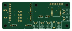 ESP8266
ESP8266ControllerCircuit
stuartpittaway
75 × 30 mm20 parts2LCC-BY-NC-4.01.1k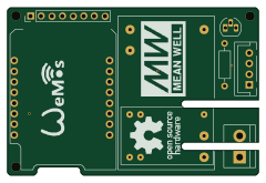 ESP8266
HASwitchPlate
aderusha
60 × 40 mm8 parts2LMIT738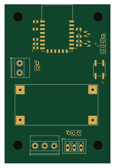 ESP8266
RatGDO-OpenSource-Bare-ESP8266
Kaldek
55 × 82.7 mm20 parts2LMIT506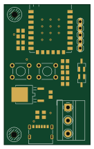 ESP8266
Goatgdo
32.9 × 53.3 mm23 parts2LMIT506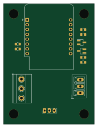 ESP8266
RatGDO-OpenSource-D1Mini-ESP8266
47.8 × 63.3 mm12 parts2LMIT506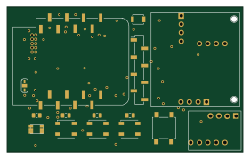 ESP8266
Iaq board
nkitanov
70.1 × 43.2 mm17 parts2LNo license398