
MainPCB V3

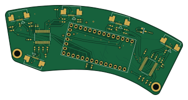
About the MainPCB V3 PCB
MainPCB V3 is an open source NXP PCB design by selina101, published on GitHub. It is a 4-layer board measuring 93.1 × 47.3 mm, with 72 components from 8 distinct parts.
Its main chip is the Teensy_4.0, from the NXP family. Other key parts include the TCA9548APWR and pad. By type, the board carries 31 ICs, 28 resistors, 7 capacitors, 5 connectors and 1 transistor.
It belongs with the sensors designs in this gallery.
From the project
Repo with projects done during my thesis and the valorisation.
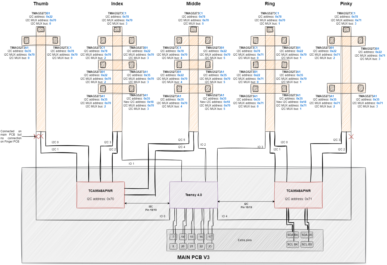
For each hand, you will need one ThumbV1 FPCB, three IndexMiddleRingV3 FPCB, one PinkyV1 and one MainPCBV3.
The hall sensors exist in three versions (with three different I2C addresses). The correct sensor placement is shown in 'FullHandDiagram.png'.
Main components on the MainPCB V3
MainPCB V3 bill of materials (BOM)
72 components, 8 distinct parts — part numbers from the project's BOM.
| Qty | Part | Footprint | Refs |
|---|---|---|---|
| 2 | TCA9548APWR | TCA9548APWR | U1, U3 |
| 1 | Teensy_4.0 | Teensy_4.0 | U2 |
| 28 | pad | pad | U4, U5, U6, U7, U8, U9, U10, U11 +20 |
| 1 | DMP31D0U-7 | DMP31D0U-7 | Q1 |
| 5 | Molex_0527450797 | Molex_0527450797 | J1, J2, J3, J4, J5 |
| 2 | 1uF | 0402_HandSolder | C1, C2 |
| 5 | 22uF | 0402_HandSolder | C3, C4, C5, C6, C7 |
| 28 | 10k | 0402_HandSolder | R1, R2, R3, R4, R5, R6, R7, R8 +20 |
MainPCB V3 design files
The KiCad project lives in the selina101/CreateLabWork repository on GitHub; these links point at the commit this page was built from.
MainPCB V3: common questions
What microcontroller does the MainPCB V3 use?
The MainPCB V3 is built around the Teensy_4.0, from the NXP family.
How big is the MainPCB V3 PCB?
The MainPCB V3 measures 93.1 × 47.3 mm, has 4 copper layers and is 1.6 mm thick.
How many components are on the MainPCB V3?
72 components, from 8 distinct parts, with part numbers taken from the project's own BOM. The full bill of materials is listed on this page.
Where can I download the MainPCB V3 design files?
From the selina101/CreateLabWork repository on GitHub, which has the KiCad layout, the schematic and the BOM; the links under Design files point to each one.
Can I use the MainPCB V3 design in my own project?
The repository has no license, so all rights stay with selina101. Use it as a reference, and ask the author before reusing the design.
Can I test firmware for the MainPCB V3 without the hardware?
Yes. HardLabs builds a simulation of the board from its netlist and BOM, so you can run and debug NXP firmware against it before you order a PCB.
More boards in CreateLabWork
 NXP
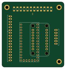
Finger FSR V1 main
57 × 60 mm37 parts2LNo license0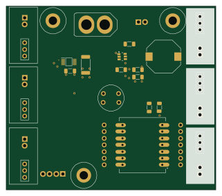 ESP32
Max Main
80 × 70 mm29 parts4LNo license0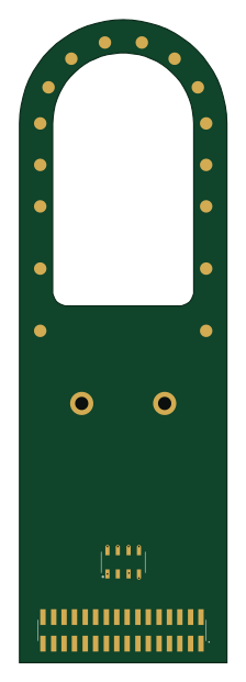
Benhui Tongue
50 × 155 mm28 parts2LNo license0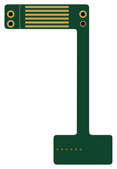
Finger FSR V1 length
55.3 × 82.3 mm24 parts2LNo license0
Index Middle Ring V3
188.9 × 26.5 mm15 parts2LNo license0
IMU6
10 × 10 mm15 parts2LNo license0
IMU V3
10 × 12 mm12 parts4LNo license0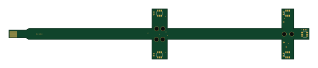
Pinky V1
157.3 × 26.5 mm11 parts2LNo license0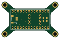 NXP
IMU Main
52.8 × 33 mm9 parts2LNo license0
Thumb V1
240.6 × 26.5 mm7 parts2LNo license0
Similar boards
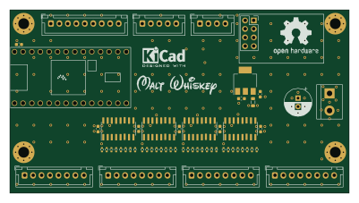 NXP
32Bit shift register
MaltWhiskey
100 × 54 mm56 parts4LNo license763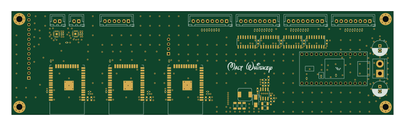 NXP
Mega-Cube-Board
200 × 54 mm100 parts4LNo license763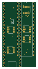 NXP
MCL6809
MicroCoreLabs
32.3 × 61 mm7 parts4LNo license532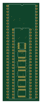 NXP
MCL68
31.6 × 84.1 mm13 parts4LNo license532 NXP
MCL65+
72.6 × 64.1 mm6 parts2LNo license532 NXP
MCLZ8
37.1 × 61.5 mm6 parts4LNo license532