
Pinky V1

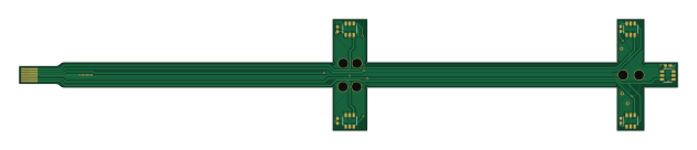
About the Pinky V1 PCB
Pinky V1 is an open source PCB design by selina101, published on GitHub. It is a 2-layer board measuring 157.3 × 26.5 mm, with 11 components from 3 distinct parts.
Other key parts include the TMAG5273A2QDBVR. By type, the board carries 6 ICs and 5 capacitors.
It belongs with the sensors designs in this gallery.
From the project
Repo with projects done during my thesis and the valorisation.
For each hand, you will need one ThumbV1 FPCB, three IndexMiddleRingV3 FPCB, one PinkyV1 and one MainPCBV3.
The hall sensors exist in three versions (with three different I2C addresses). The correct sensor placement is shown in 'FullHandDiagram.png'.
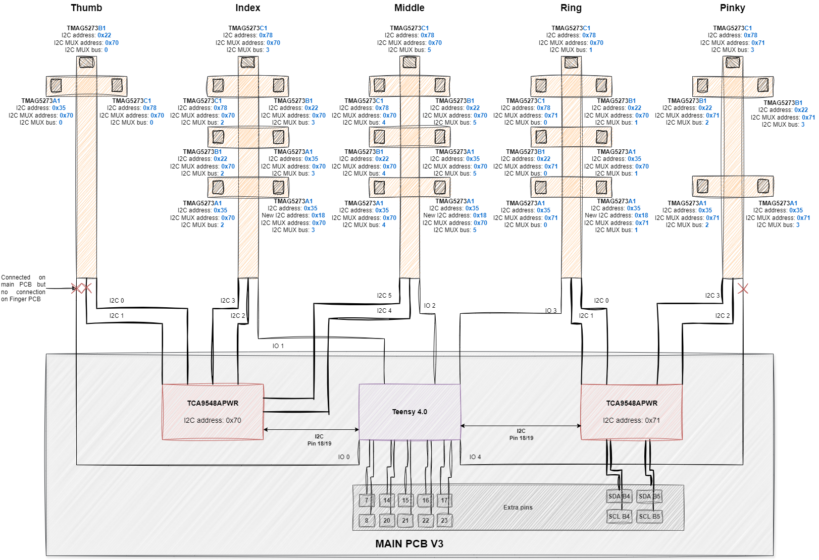
Main components on the Pinky V1
Pinky V1 bill of materials (BOM)
11 components, 3 distinct parts — part numbers from the project's BOM.
| Qty | Part | Footprint | Refs |
|---|---|---|---|
| 5 | TMAG5273A2QDBVR | TMAG5273A2 | U1, U2, U3, U4, U5 |
| 1 | ~ | 7Pin_FingerConnector_for 0527450797 | U8 |
| 5 | 0.1uF | C_0402_1005Metric_Pad0.74x0.62mm_HandSolder | C1, C2, C3, C4, C5 |
Pinky V1 design files
The KiCad project lives in the selina101/CreateLabWork repository on GitHub; these links point at the commit this page was built from.
Pinky V1: common questions
How big is the Pinky V1 PCB?
The Pinky V1 measures 157.3 × 26.5 mm, has 2 copper layers and is 1.6 mm thick.
How many components are on the Pinky V1?
11 components, from 3 distinct parts, with part numbers taken from the project's own BOM. The full bill of materials is listed on this page.
Where can I download the Pinky V1 design files?
From the selina101/CreateLabWork repository on GitHub, which has the KiCad layout, the schematic and the BOM; the links under Design files point to each one.
Can I use the Pinky V1 design in my own project?
The repository has no license, so all rights stay with selina101. Use it as a reference, and ask the author before reusing the design.
More boards in CreateLabWork
 NXP
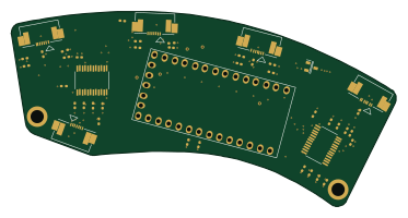
MainPCB V3
93.1 × 47.3 mm72 parts4LNo license0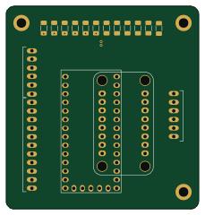 NXP
Finger FSR V1 main
57 × 60 mm37 parts2LNo license0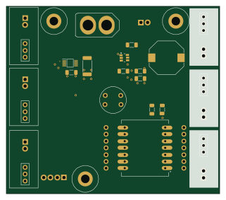 ESP32
Max Main
80 × 70 mm29 parts4LNo license0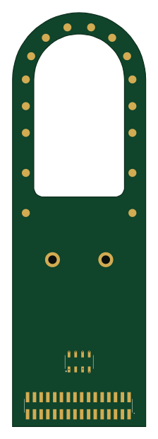
Benhui Tongue
50 × 155 mm28 parts2LNo license0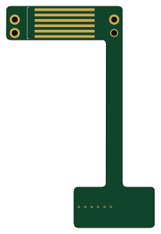
Finger FSR V1 length
55.3 × 82.3 mm24 parts2LNo license0
Index Middle Ring V3
188.9 × 26.5 mm15 parts2LNo license0
IMU6
10 × 10 mm15 parts2LNo license0
IMU V3
10 × 12 mm12 parts4LNo license0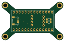 NXP
IMU Main
52.8 × 33 mm9 parts2LNo license0
Thumb V1
240.6 × 26.5 mm7 parts2LNo license0
Similar boards
Sensor smd
scottbez1
40 × 20 mm5 parts2LApache-2.04.2k
Sensors
StuckAtPrototype
15.2 × 9 mm14 parts4LApache-2.03.8k
Microphone
Mentra-Community
5.5 × 6.1 mm6 parts2LMIT1.2k
TemperaturePCB PANEL
stuartpittaway
116 × 75.5 mm178 parts2LCC-BY-NC-4.01.1k
Pots
shanteacontrols
390 × 93 mm75 parts2LApache-2.0956
USB
52 × 12.6 mm6 parts2LApache-2.0956