
Tapeshnik proto

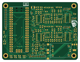
About the Tapeshnik proto PCB
Tapeshnik proto is an open source RP2040/RP2350 PCB design by svofski, published on GitHub. It is a 2-layer board measuring 84.3 × 64.5 mm, with 132 components from 54 distinct parts.
Its main chip is the Pico, from the RP2040/RP2350 family. Other key parts include the 74HC14, 74HC4052D, LM358, AMS1117-5.0 and REF3030. By type, the board carries 65 resistors, 25 capacitors, 12 ICs, 10 connectors, 8 transistors and 8 diodes.
From the project
compact cassette data drive
Project goals. Not all of them are realistic.
utilize an existing consumer tape mechanism with "logic control" to make a fully automatic tape drive investigate the limits of what can be done with a simple compact cassette implement random access to sectors a usb mass storage device use a stereo track for double data rate access, eventually use a 4-track head for quad data rate investigate if altering motor speed to improve r/w speeds makes sense * investigate feasibility of reading while fast-forwarding with heads half-lifted
Main components on the Tapeshnik proto
Tapeshnik proto bill of materials (BOM)
132 components, 54 distinct parts — part numbers from the project's BOM.
| Qty | Part | Footprint | Refs |
|---|---|---|---|
| 1 | Pico | RPi_Pico_SMD_TH | U1 |
| 2 | 74HC14 | SOIC-14_3.9x8.7mm_P1.27mm | U2, U9 |
| 2 | 74HC4052D | SO-16_3.9x9.9mm_P1.27mm | U3, U6 |
| 4 | LM358 | SO-8_3.9x4.9mm_P1.27mm | U4, U5, U8, U10 |
| 1 | AMS1117-5.0 | SOT-223-3_TabPin2 | U7 |
| 1 | REF3030 | SOT-23 | U11 |
| 1 | SPX3819M5-L-5-0 | SOT-23-5 | U12 |
| 4 | AO3400 | SOT-23 | Q1, Q2, Q4, Q6 |
| 1 | S8050 | SOT-23 | Q3 |
| 1 | AP3101 AO3401 | SOT-23 | Q5 |
| 1 | S8050 | SOT-23 | Q7 |
| 1 | AO3401 | SOT-23 | Q8 |
| 1 | Conn_01x02 | PinHeader_1x02_P2.54mm_Vertical | J1 |
| 2 | RW_HEAD | PinHeader_1x03_P2.54mm_Vertical | J2, J5 |
| 1 | Conn_01x07 | PinHeader_1x07_P2.54mm_Vertical | J3 |
| 1 | ERASERHEAD | PinHeader_1x02_P2.54mm_Vertical | J4 |
| 4 | Conn_01x01_Pin | PinHeader_1x01_P2.54mm_Vertical | J6, J7, J8, J9 |
| 1 | Conn_01x09 | PinHeader_1x09_P2.54mm_Vertical | J10 |
| 2 | SolderJumper_2_Bridged | SolderJumper-2_P1.3mm_Bridged2Bar_Pad1.0x1.5mm | JP1, JP2 |
| 2 | Conn_01x01_Pin | PinHeader_1x01_P2.54mm_Vertical | TP1, TP2 |
Show 34 more
| Qty | Part | Footprint | Refs |
|---|---|---|---|
| 4 | BAT54S | SOT-23 | D1, D2, D3, D4 |
| 1 | red | LED_0603_1608Metric | D5 |
| 2 | green | LED_0603_1608Metric | D6, D7 |
| 1 | orange | LED_0603_1608Metric | D8 |
| 5 | 0.1U 0.1u | C_0805_2012Metric | C1, C5, C11, C15, C22 |
| 2 | 180P 180p | C_0805_2012Metric | C2, C12 |
| 2 | 2000P 2200p | C_0805_2012Metric | C3, C13 |
| 2 | 150P 150p | C_0805_2012Metric | C4, C14 |
| 5 | 10.0U/25V 10.0u/25V | C_0805_2012Metric | C6, C7, C17, C18, C21 |
| 6 | 0.1U 0.1u | C_0603_1608Metric | C8, C9, C10, C16, C19, C20 |
| 1 | 220.0/16V | CP_EIA-7343-31_Kemet-D | C23 |
| 1 | 47.0/16V | CP_EIA-3528-21_Kemet-B | C24 |
| 1 | 220.0/16V | CP_EIA-7343-31_Kemet-D | C25 |
| 4 | 100K | R_0805_2012Metric | R1, R12, R32, R37 |
| 4 | 47 | R_0805_2012Metric | R2, R3, R62, R63 |
| 1 | 22K | R_0805_2012Metric | R4 |
| 10 | 10K | R_0805_2012Metric | R5, R8, R9, R22, R24, R34, R35, R36 +2 |
| 7 | 470 | R_0805_2012Metric | R6, R7, R30, R31, R38, R40, R60 |
| 4 | 330K | R_0805_2012Metric | R10, R17, R39, R46 |
| 6 | 2K7 | R_0805_2012Metric | R11, R16, R21, R41, R45, R50 |
| 2 | 6K8 | R_0805_2012Metric | R13, R42 |
| 6 | 47K | R_0805_2012Metric | R14, R15, R20, R43, R44, R48 |
| 2 | 3K9 | R_0805_2012Metric | R18, R47 |
| 2 | 56K | R_0805_2012Metric | R19, R49 |
| 2 | 2M2 | R_0805_2012Metric | R23, R55 |
| 3 | 1K | R_0805_2012Metric | R25, R29, R56 |
| 1 | 3K3 | R_0805_2012Metric | R26 |
| 1 | 2K2 | R_0805_2012Metric | R27 |
| 1 | 220 | R_0805_2012Metric | R28 |
| 4 | N/C | R_0805_2012Metric | R33, R57, R58, R59 |
| 2 | 4K7 | R_0805_2012Metric | R53, R54 |
| 1 | 760 680 | R_0805_2012Metric | R61 |
| 1 | 22K | R_0805_2012Metric | R64 |
| 1 | 4K7 | R_0805_2012Metric | R66 |
Tapeshnik proto design files
The KiCad project lives in the svofski/tapeshnik repository on GitHub; these links point at the commit this page was built from.
Tapeshnik proto: common questions
What microcontroller does the Tapeshnik proto use?
The Tapeshnik proto is built around the Pico, from the RP2040/RP2350 family.
How big is the Tapeshnik proto PCB?
The Tapeshnik proto measures 84.3 × 64.5 mm, has 2 copper layers and is 1.6 mm thick.
How many components are on the Tapeshnik proto?
132 components, from 54 distinct parts, with part numbers taken from the project's own BOM. The full bill of materials is listed on this page.
Where can I download the Tapeshnik proto design files?
From the svofski/tapeshnik repository on GitHub, which has the KiCad layout, the schematic and the BOM; the links under Design files point to each one.
Can I use the Tapeshnik proto design in my own project?
The repository has no license, so all rights stay with svofski. Use it as a reference, and ask the author before reusing the design.
Can I test firmware for the Tapeshnik proto without the hardware?
Yes. HardLabs builds a simulation of the board from its netlist and BOM, so you can run and debug RP2040/RP2350 firmware against it before you order a PCB.
More boards in tapeshnik

Similar boards
 RP2040/RP2350
Open Book Abridged Edition
joeycastillo
85 × 115 mm29 parts2LCC-BY-SA-4.08.1k RP2040/RP2350
Corne
foostan
277.2 × 107.5 mm164 parts2LCC-BY-4.07.7k RP2040/RP2350
Corne
277.2 × 107.5 mm164 parts2LCC-BY-4.07.7k RP2040/RP2350
LogicAnalyzer
gusmanb
57 × 55.2 mm6 parts2LGPL-3.05.0k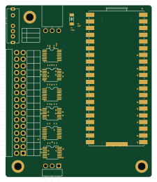 RP2040/RP2350
Jitx design
55.5 × 65 mm26 parts4LGPL-3.05.0k RP2040/RP2350
Main
google
98 × 71 mm102 parts2LApache-2.02.9k