
Device Board

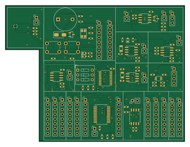
About the Device Board
Device Board is an open source PCB design by WestianPKl, published on GitHub. It is a 2-layer board measuring 94.7 × 71.8 mm, with 104 components from 46 distinct parts.
Other key parts include the MX25L25673GM2I-08G, MCP7940N-I/SN, FM24CL16B-GTR, PCA9306DCUR and PCF8563T. By type, the board carries 37 resistors, 19 capacitors, 17 connectors, 10 ICs, 8 jumpers and 6 diodes.
It belongs with the power & battery designs in this gallery.
From the project
A collection of custom PCB designs created in KiCAD, centered around the Raspberry Pi Pico (RP2040) platform. Each board is a standalone module that connects to the Main Board and extends its functionality via I2C, SPI, or UART.
A collection of custom PCB designs created in KiCAD, centered around the Raspberry Pi Pico (RP2040) platform. Each board is a standalone module that connects to the Main Board and extends its functionality via I2C, SPI, or UART.
Author: Piotr Kłyś Tool: KiCAD 8.x Firmware: MicroPython (Pico boards), AVR-GCC (ATmega boards)
The central development and integration board built around the Raspberry Pi Pico. Used to test all peripheral modules in the collection.
Main components on the Device Board
Device Board bill of materials (BOM)
104 components, 46 distinct parts.
| Qty | Part | Footprint | Refs |
|---|---|---|---|
| 1 | MX25L25673GM2I-08G | SOIC-8_5.3x5.3mm_P1.27mm | U1 |
| 1 | MCP7940N-I/SN | SOIC-8_3.9x4.9mm_P1.27mm | U2 |
| 1 | FM24CL16B-GTR | SOIC-8_3.9x4.9mm_P1.27mm | U3 |
| 1 | PCA9306DCUR | VSSOP-8_2.3x2mm_P0.5mm | U4 |
| 1 | PCF8563T | SOIC-8_3.9x4.9mm_P1.27mm | U5 |
| 1 | M24C32-WMN6TP | SOIC-8_3.9x4.9mm_P1.27mm | U6 |
| 1 | SHT4x | Sensirion_DFN-4_1.5x1.5mm_P0.8mm_SHT4x_NoCentralPad | U7 |
| 1 | MCP23017x-x-SS | SSOP-28_5.3x10.2mm_P0.65mm | U8 |
| 1 | TCA9548APWR | TSSOP-24_4.4x7.8mm_P0.65mm | U9 |
| 1 | SN65HVD230DR | SOIC-8_3.9x4.9mm_P1.27mm | U10 |
| 1 | BC817-40-DIO | SOT-23 | Q1 |
| 1 | QT3CD-32.768KEZF-T | Crystal_SMD_3215-2Pin_3.2x1.5mm | Y1 |
| 1 | QT3CD-32.768KEZY-T | Crystal_SMD_3215-2Pin_3.2x1.5mm | Y2 |
| 2 | +3.3V | PinHeader_1x08_P2.54mm_Vertical | J1, J3 |
| 1 | MISO | PinHeader_1x08_P2.54mm_Vertical | J2 |
| 1 | MOSI | PinHeader_1x08_P2.54mm_Vertical | J4 |
| 1 | GND | PinHeader_1x08_P2.54mm_Vertical | J5 |
| 1 | SDA | PinHeader_1x08_P2.54mm_Vertical | J6 |
| 1 | SCK | PinHeader_1x08_P2.54mm_Vertical | J7 |
| 1 | SCL | PinHeader_1x08_P2.54mm_Vertical | J8 |
Show 26 more
| Qty | Part | Footprint | Refs |
|---|---|---|---|
| 2 | Pin | PinHeader_1x08_P2.54mm_Vertical | J9, J11 |
| 1 | TX | PinHeader_1x08_P2.54mm_Vertical | J10 |
| 1 | RX | PinHeader_1x08_P2.54mm_Vertical | J12 |
| 1 | GPA | PinHeader_1x08_P2.54mm_Vertical | J13 |
| 1 | GPB | PinHeader_1x08_P2.54mm_Vertical | J14 |
| 1 | LCD 16x2 | PinHeader_1x04_P2.54mm_Vertical | J15 |
| 1 | CAN | PinHeader_1x02_P2.54mm_Vertical | J16 |
| 1 | CAN | PinHeader_1x03_P2.54mm_Vertical | J17 |
| 1 | Buzzer 5V 12mm | Buzzer_12x9.5RM7.6 | BZ1 |
| 8 | Jumper_2_Bridged | PinHeader_1x02_P2.54mm_Vertical | JP1, JP2, JP3, JP4, JP5, JP6, JP7, JP8 |
| 1 | SW_DIP_x03 | SW_DIP_SPSTx03_Slide_9.78x9.8mm_W7.62mm_P2.54mm | SW1 |
| 2 | Tact Switch 6x6mm / 13mm | SW_PUSH_6mm | SW2, SW3 |
| 3 | LED | LED_0603_1608Metric | D1, D4, D5 |
| 1 | ESDCAN01-2BLY | SOT-23 | D2 |
| 1 | M7-DIO | D_SMA | D3 |
| 1 | OSTBPCS2C2B | LED_Avago_PLCC4_3.2x2.8mm_CW | D6 |
| 14 | 100nF | C_0603_1608Metric | C1, C3, C4, C5, C6, C7, C10, C11 +6 |
| 2 | 1uF | C_0603_1608Metric | C2, C14 |
| 2 | 12pF | C_0603_1608Metric | C8, C9 |
| 1 | 4.7nF | C_0603_1608Metric | C16 |
| 4 | 10kR | R_0603_1608Metric | R1, R2, R9, R14 |
| 14 | 4k7R | R_0603_1608Metric | R3, R4, R5, R6, R7, R8, R10, R11 +6 |
| 11 | 47kR | R_0603_1608Metric | R15, R16, R17, R18, R23, R24, R25, R26 +3 |
| 2 | 60R | R_0603_1608Metric | R30, R31 |
| 3 | 1kR | R_0603_1608Metric | R32, R36, R37 |
| 3 | 220R | R_0603_1608Metric | R33, R34, R35 |
Device Board design files
The KiCad project lives in the WestianPKl/pcb-docs repository on GitHub; these links point at the commit this page was built from.
Device Board: common questions
How big is the Device Board?
The Device Board measures 94.7 × 71.8 mm, has 2 copper layers and is 1.6 mm thick.
How many components are on the Device Board?
104 components, from 46 distinct parts. The full bill of materials is listed on this page.
Where can I download the Device Board design files?
From the WestianPKl/pcb-docs repository on GitHub, which has the KiCad layout and the schematic; the links under Design files point to each one.
Can I use the Device Board design in my own project?
The repository has no license, so all rights stay with WestianPKl. Use it as a reference, and ask the author before reusing the design.
More boards in pcb-docs
 ESP32
IoT Logger B
94.7 × 71.8 mm135 parts2LNo license0 STM32
STM Board
74.1 × 91.8 mm127 parts4LNo license0 STM32
Tree Board
160 × 158 mm117 parts2LNo license0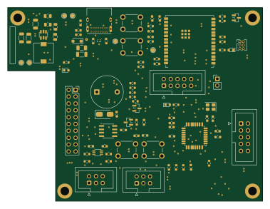 ESP32
IoT Logger C
94.7 × 71.8 mm97 parts2LNo license0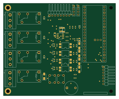 Raspberry Pi
 Pico Logger - Relay
100.5 × 83 mm77 parts2LNo license0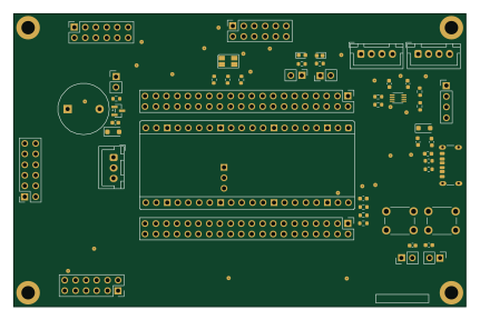 RP2040/RP2350
Main Board
107.5 × 69.8 mm51 parts2LNo license0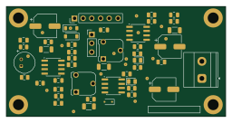
Amplifier Board
64 × 32.1 mm46 parts2LNo license0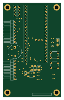 RP2040/RP2350
Raspberry Pi Pico Logger
51.5 × 83 mm33 parts2LNo license0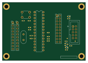 AVR/Arduino
ATMega Board
71.7 × 50.2 mm24 parts2LNo license0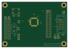 AVR/Arduino
ATMegaSMD Board
71.7 × 50.2 mm24 parts2LNo license0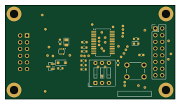
GPIO Board
64.2 × 35.6 mm21 parts2LNo license0
Similar boards
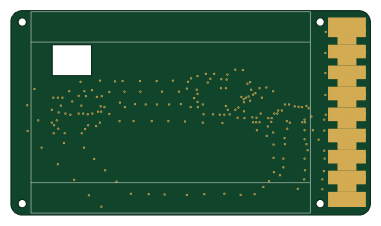
EinkPDA screen
TalismanDesign
95 × 54 mm27 parts2LApache-2.02.0k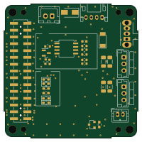
Stack chan
stack-chan
50 × 50 mm33 parts2LApache-2.01.7k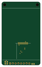
Display Carrier
AxxAxx
35.6 × 58.2 mm5 parts2LGPL-3.01.7k
ProgrammingAdapter
stuartpittaway
10.5 × 83 mm3 parts2LCC-BY-NC-4.01.1k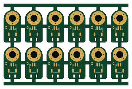
TemperaturePCB PANEL
116 × 75.5 mm178 parts2LCC-BY-NC-4.01.1k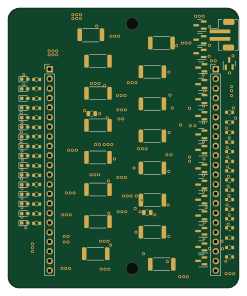
Module 16S PassiveBalanceAddOn
61 × 74 mm86 parts2LCC-BY-NC-4.01.1k