
Before width normalization

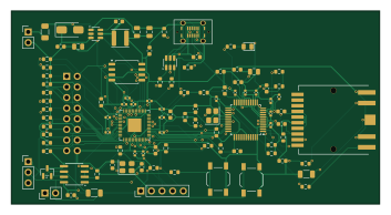
About the Before width normalization PCB
Before width normalization is an open source RP2040/RP2350 PCB design by beleata, published on GitHub. It is a 2-layer board measuring 88 × 46.1 mm, with 103 components from 46 distinct parts.
Its main chip is the RP2040, from the RP2040/RP2350 family. Other key parts include the W25Q64JVSSIQ, USBLC6-2SC6, AP63203WU-7, SN65HVD75DR and W5500. By type, the board carries 42 capacitors, 38 resistors, 6 ICs, 6 connectors, 3 diodes and 2 crystals.
From the project
iCE40HX1K 64x32 ICND1065L RGB panel with double-buffered SRAM and 2 Mbaud UART image upload
Development snapshot, 2026-09-25. NOT FOR MANUFACTURE.
A custom two-layer 88 x 46.1 mm controller for the tested 64 x 32 ICND1065L LED panel. Bare RP2040, 8 MiB flash, vertical USB-C, non-isolated RS-485, W5500 Ethernet and a vertical HanRun HR963380AE integrated-magnetics jack. KiCad 10.0.6 project, 103 components. The custom PCB has not been fabricated or tested; the working YD-RP2040 module firmware is a separate result.
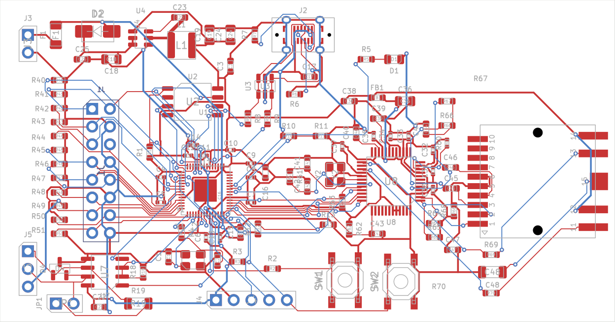
Main components on the Before width normalization
Before width normalization bill of materials (BOM)
103 components, 46 distinct parts — part numbers from the project's BOM.
| Qty | Part | Footprint | Refs |
|---|---|---|---|
| 1 | RP2040 | QFN-56-1EP_7x7mm_P0.4mm_EP3.2x3.2mm | U1 |
| 1 | W25Q64JVSSIQ | SOIC-8_5.3x5.3mm_P1.27mm | U2 |
| 1 | USBLC6-2SC6 | SOT-23-6 | U3 |
| 1 | AP63203WU-7 | TSOT-23-6 | U4 |
| 1 | SN65HVD75DR | SOIC-8_3.9x4.9mm_P1.27mm | U7 |
| 1 | W5500 | LQFP-48_7x7mm_P0.5mm | U8 |
| 1 | C20625731 ABM8-272-T3 12MHz | Crystal_SMD_3225-4Pin_3.2x2.5mm | Y1 |
| 1 | ABM8-25.000MHZ-D2Y-T | Crystal_SMD_3225-4Pin_3.2x2.5mm | Y2 |
| 1 | PANEL BOTTOM 2x8 | PinSocket_2x08_P2.54mm_Vertical | J1 |
| 1 | C3151748 USB-C VERTICAL H6.5 | USB_C_SHOUHAN_TYPE-C_16PLT-H6.5_Vertical | J2 |
| 1 | PANEL POWER +5V GND | PinHeader_1x02_P2.54mm_Vertical | J3 |
| 1 | SWD 3V3 GND CLK IO RUN | PinHeader_1x05_P2.54mm_Vertical | J4 |
| 1 | RS485 A B GND | PinHeader_1x03_P2.54mm_Vertical | J5 |
| 1 | C19724763 HR963380AE MAGJACK | RJ45_HanRun_HR963380AE_Vertical | J6 |
| 1 | C70076 PTC 0.5A | Fuse_1206_3216Metric | F1 |
| 1 | TERM 120R | PinHeader_1x02_P2.54mm_Vertical | JP1 |
| 1 | BOOTSEL | SW_SPST_TL3342 | SW1 |
| 1 | RESET | SW_SPST_TL3342 | SW2 |
| 1 | C2297 STATUS green | LED_0805_2012Metric | D1 |
| 1 | SS14 | D_SMA | D2 |
Show 26 more
| Qty | Part | Footprint | Refs |
|---|---|---|---|
| 1 | SM712 | SOT-23 | D4 |
| 1 | C14709 120R@100MHz 2A | L_0603_1608Metric | FB1 |
| 1 | C96899 3.9u SWPA4030S3R9MT | L_Sunlord_SWPA4030S | L1 |
| 2 | 15P 15p | C_0603_1608Metric | C1, C2 |
| 6 | 100N 100n | C_0603_1608Metric | C3, C22, C23, C25, C43, C47 |
| 18 | 100N 100n | C_0402_1005Metric | C4, C5, C6, C7, C8, C9, C10, C11 +10 |
| 3 | 1u | C_0603_1608Metric | C15, C16, C17 |
| 2 | C1713 10u 16V | C_0805_2012Metric | C18, C36 |
| 2 | C29277 22u 10V | C_0805_2012Metric | C19, C24 |
| 2 | 4.7U 4.7u | C_0603_1608Metric | C38, C39 |
| 2 | 10N 10n | C_0603_1608Metric | C40, C44 |
| 2 | C1656 27p C0G | C_0603_1608Metric | C41, C42 |
| 2 | 6.8N 6.8n | C_0603_1608Metric | C45, C46 |
| 1 | C1941 1n 1kV | C_1206_3216Metric | C48 |
| 5 | 10K 10k | R_0603_1608Metric | R1, R3, R18, R62, R63 |
| 3 | 1k | R_0603_1608Metric | R2, R4, R5 |
| 2 | 5.1K 5.1k | R_0603_1608Metric | R6, R7 |
| 2 | 27 | R_0603_1608Metric | R8, R9 |
| 4 | 100K 100k | R_0603_1608Metric | R10, R11, R12, R13 |
| 1 | C17909 120 0.25W | R_1206_3216Metric | R19 |
| 12 | 47K 47k | R_0603_1608Metric | R40, R41, R42, R43, R44, R45, R46, R47 +4 |
| 1 | C11692 12.4k 1% | R_0402_1005Metric | R60 |
| 1 | 1M | R_0603_1608Metric | R61 |
| 4 | C23185 49.9 1% | R_0603_1608Metric | R64, R65, R66, R67 |
| 1 | 10 | R_0603_1608Metric | R68 |
| 2 | 470 | R_0603_1608Metric | R69, R70 |
Before width normalization design files
The KiCad project lives in the beleata/fpga-led-panel-sram repository on GitHub; these links point at the commit this page was built from.
Before width normalization: common questions
What microcontroller does the Before width normalization use?
The Before width normalization is built around the RP2040, from the RP2040/RP2350 family.
How big is the Before width normalization PCB?
The Before width normalization measures 88 × 46.1 mm, has 2 copper layers and is 0.8 mm thick.
How many components are on the Before width normalization?
103 components, from 46 distinct parts, with part numbers taken from the project's own BOM. The full bill of materials is listed on this page.
Where can I download the Before width normalization design files?
From the beleata/fpga-led-panel-sram repository on GitHub, which has the KiCad layout and the BOM; the links under Design files point to each one.
Can I use the Before width normalization design in my own project?
The repository has no license, so all rights stay with beleata. Use it as a reference, and ask the author before reusing the design.
Can I test firmware for the Before width normalization without the hardware?
Yes. HardLabs builds a simulation of the board from its netlist and BOM, so you can run and debug RP2040/RP2350 firmware against it before you order a PCB.
More boards in fpga-led-panel-sram
 RP2040/RP2350
Pico panel
88 × 46.1 mm103 parts2LNo license0 RP2040/RP2350
First pass
88 × 46.1 mm103 parts2LNo license0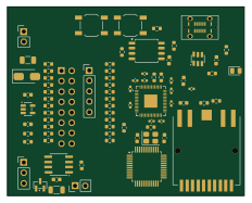 RP2040/RP2350
Ethernet fit plot
57.8 × 46.1 mm79 parts2LNo license0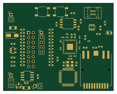 RP2040/RP2350
Ethernet mechanical
57.8 × 46.1 mm79 parts2LNo license0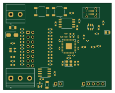 RP2040/RP2350
Placement review
57.8 × 46.1 mm77 parts2LNo license0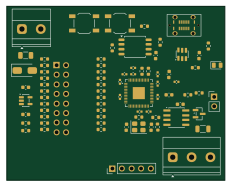 RP2040/RP2350
Placement before rs485-move
57.8 × 46.1 mm77 parts2LNo license0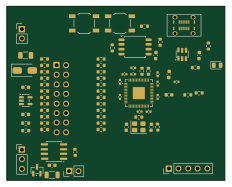 RP2040/RP2350
Placement review plot
57.8 × 46.1 mm77 parts2LNo license0
Similar boards
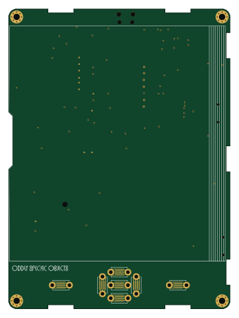 RP2040/RP2350
Open Book Abridged Edition
joeycastillo
85 × 115 mm29 parts2LCC-BY-SA-4.08.1k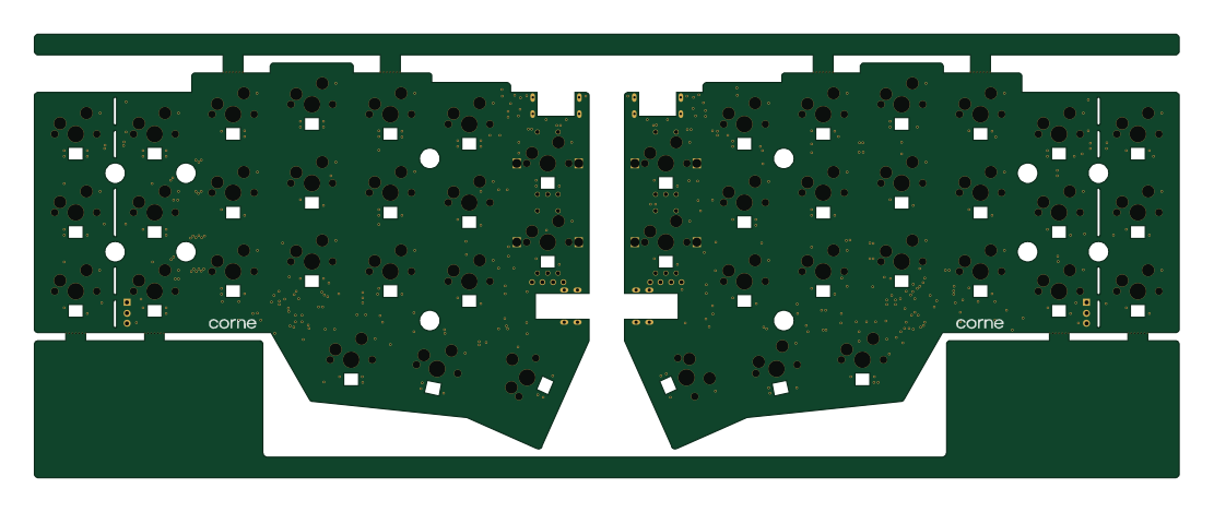 RP2040/RP2350
Corne
foostan
277.2 × 107.5 mm164 parts2LCC-BY-4.07.7k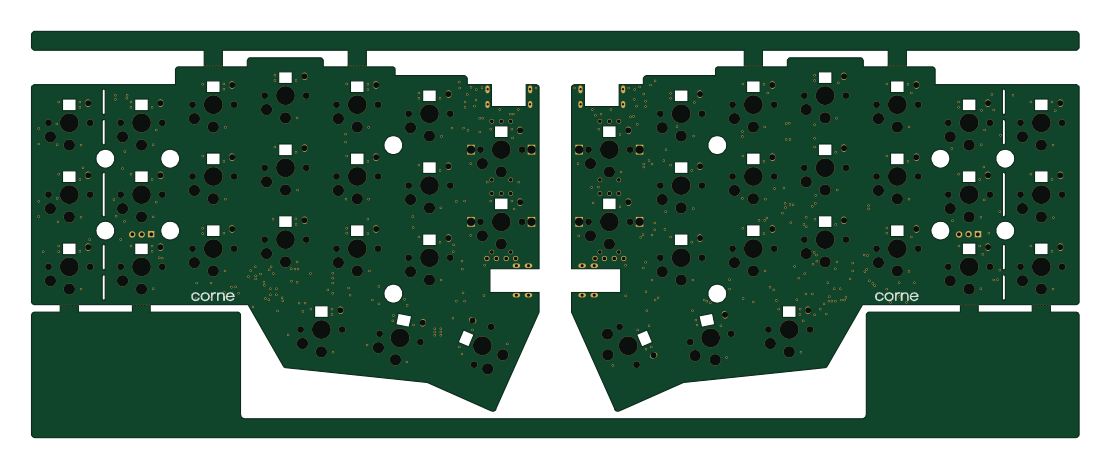 RP2040/RP2350
Corne
277.2 × 107.5 mm164 parts2LCC-BY-4.07.7k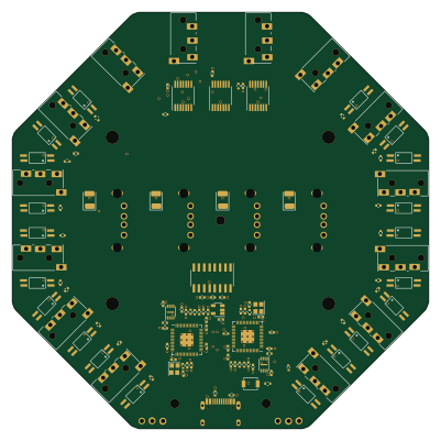 RP2040/RP2350
Hid remapper
jfedor2
100 × 100 mm124 parts2LMIT1.7k RP2040/RP2350
Msa
Mentra-Community
47.8 × 9.4 mm53 parts2LMIT1.2k RP2040/RP2350
Open Source Smart Glasses
93 × 10.5 mm80 parts4LMIT1.2k