
BackplaneTest

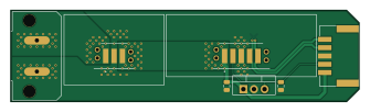
About the BackplaneTest PCB
BackplaneTest is an open source PCB design by berkeleyauv, published on GitHub under the GPL-3.0 license. It is a 2-layer board measuring 83.5 × 22 mm, with 8 components from 7 distinct parts.
Other key parts include the LM7805_TO220. By type, the board carries 4 connectors, 2 capacitors, 1 IC and 1 resistor.
It belongs with the robotics & motion designs in this gallery.
From the project
PCB designs for Underwater Robotics at Berkeley (UR@B)
Tests the ESCC and PCC along with a Molex Super Sabre for power.
Main components on the BackplaneTest
BackplaneTest bill of materials (BOM)
8 components, 7 distinct parts.
| Qty | Part | Footprint | Refs |
|---|---|---|---|
| 1 | LM7805_TO220 | TO-220-3_Vertical | U1 |
| 1 | Power | Molex_SuperSabre_Vert_2pin | J1 |
| 1 | PCC | Samtec_mPOWER_UMPS_3pin | J2 |
| 1 | ESCC | Samtec_mPOWER_UMPS_5pin | J3 |
| 1 | CAN | Molex_DuraClik_RH_5pin | J4 |
| 2 | 10u | C_0805_2012Metric | C1, C2 |
| 1 | 120 | R_0603_1608Metric | R1 |
BackplaneTest design files
The KiCad project lives in the berkeleyauv/RoboSub_HW repository on GitHub; these links point at the commit this page was built from.
BackplaneTest: common questions
How big is the BackplaneTest PCB?
The BackplaneTest measures 83.5 × 22 mm, has 2 copper layers and is 1.6 mm thick.
How many components are on the BackplaneTest?
8 components, from 7 distinct parts. The full bill of materials is listed on this page.
Where can I download the BackplaneTest design files?
From the berkeleyauv/RoboSub_HW repository on GitHub, which has the KiCad layout and the schematic; the links under Design files point to each one.
Can I use the BackplaneTest design in my own project?
Yes, under the terms of its GPL-3.0 license, which berkeleyauv chose for the repository.
More boards in RoboSub_HW
 STM32
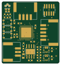
STM32NOGGIN
31.3 × 34 mm57 parts4LGPL-3.03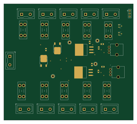
Power distribution board
115.6 × 104.1 mm41 parts2LGPL-3.03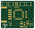 STM32
STM32NOGUSB
30.5 × 25 mm34 parts2LGPL-3.03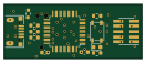 STM32
STM32NOGPROG
33 × 13 mm33 parts2LGPL-3.03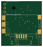 STM32
STM32ESCC
36 × 40 mm28 parts2LGPL-3.03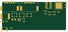 STM32
STM32Noggin f072cb
59 × 25.9 mm26 parts2LGPL-3.03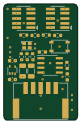
NOGLINK
19.5 × 30.8 mm22 parts2LGPL-3.03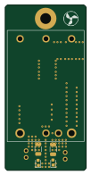
PCC
24 × 49 mm22 parts2LGPL-3.03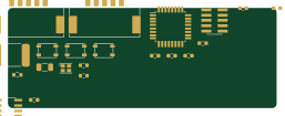 STM32
STM32Noggin g0b1ke
64.3 × 24 mm21 parts2LGPL-3.03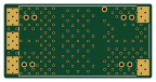
ESCB
36 × 18 mm8 parts2LGPL-3.03
Similar boards

Stack chan
stack-chan
50 × 50 mm33 parts2LApache-2.01.7k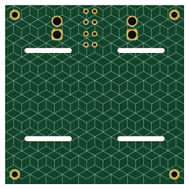
Cube batteryboard
willem-pennings
95 × 95 mm4 parts2LGPL-3.01.1k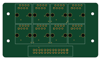
Mesabob
rene-dev
87.5 × 50 mm44 parts2LGPL-3.0979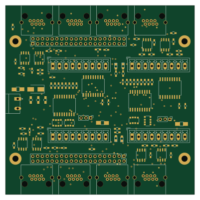
Bob
100 × 100 mm140 parts2LGPL-3.0979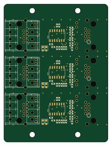
Triple adapter
57 × 75 mm26 parts2LGPL-3.0979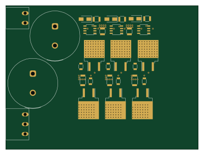
Trollerv2
100 × 75 mm33 parts4LGPL-3.0979