
NOGLINK

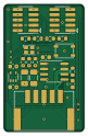
About the NOGLINK PCB
NOGLINK is an open source PCB design by berkeleyauv, published on GitHub under the GPL-3.0 license. It is a 2-layer board measuring 19.5 × 30.8 mm, with 22 components from 15 distinct parts.
Other key parts include the MIC5365-3.3YC5, STLINK-V3MODS and ATA6561. By type, the board carries 8 resistors, 4 capacitors, 3 ICs, 3 connectors, 2 fuses and 1 switch.
It belongs with the robotics & motion designs in this gallery.
From the project
PCB designs for Underwater Robotics at Berkeley (UR@B)
Carrier for STLINK-V3MODS with CAN transceiver, button, RGB LED, SWD, UART, and stbridge breakout.
Main components on the NOGLINK
NOGLINK bill of materials (BOM)
22 components, 15 distinct parts.
| Qty | Part | Footprint | Refs |
|---|---|---|---|
| 1 | MIC5365-3.3YC5 | SOT-353_SC-70-5 | U1 |
| 1 | STLINK-V3MODS | STLINK-V3MODS | U2 |
| 1 | ATA6561 | SOIC-8_3.9x4.9mm_P1.27mm | U3 |
| 1 | CAN | Molex_DuraClik_RH_5pin | J1 |
| 1 | SWD/VCP | PinHeader_2x05_P1.27mm_Vertical_SMD | J2 |
| 1 | SPI/I2C/UART | PinHeader_2x05_P1.27mm_Vertical_SMD | J3 |
| 2 | 500mA | Fuse_1206_3216Metric | F1, F2 |
| 1 | USR | SW_SPST_PTS810 | SW1 |
| 1 | LED_ARGB | LED_Cree-PLCC4_2x2mm_CW | D1 |
| 2 | 1u | C_0603_1608Metric | C1, C2 |
| 2 | 100n | C_0603_1608Metric | C3, C4 |
| 1 | 120 | R_0603_1608Metric | R1 |
| 2 | 0 | R_0603_1608Metric | R2, R6 |
| 3 | 47 | R_0603_1608Metric | R3, R4, R5 |
| 2 | 2.2k | R_0603_1608Metric | R7, R8 |
NOGLINK design files
The KiCad project lives in the berkeleyauv/RoboSub_HW repository on GitHub; these links point at the commit this page was built from.
NOGLINK: common questions
How big is the NOGLINK PCB?
The NOGLINK measures 19.5 × 30.8 mm, has 2 copper layers and is 1.6 mm thick.
How many components are on the NOGLINK?
22 components, from 15 distinct parts. The full bill of materials is listed on this page.
Where can I download the NOGLINK design files?
From the berkeleyauv/RoboSub_HW repository on GitHub, which has the KiCad layout and the schematic; the links under Design files point to each one.
Can I use the NOGLINK design in my own project?
Yes, under the terms of its GPL-3.0 license, which berkeleyauv chose for the repository.
More boards in RoboSub_HW
 STM32
STM32NOGGIN
31.3 × 34 mm57 parts4LGPL-3.03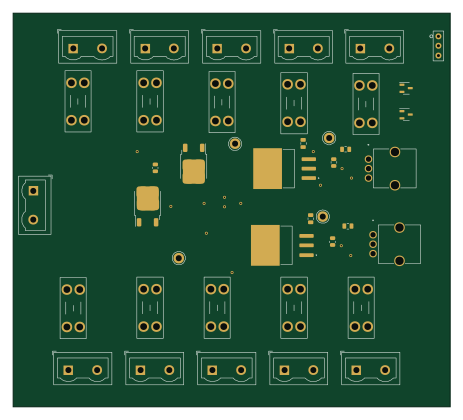
Power distribution board
115.6 × 104.1 mm41 parts2LGPL-3.03 STM32
STM32NOGUSB
30.5 × 25 mm34 parts2LGPL-3.03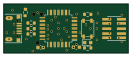 STM32
STM32NOGPROG
33 × 13 mm33 parts2LGPL-3.03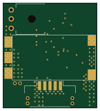 STM32
STM32ESCC
36 × 40 mm28 parts2LGPL-3.03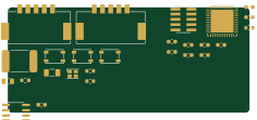 STM32
STM32Noggin f072cb
59 × 25.9 mm26 parts2LGPL-3.03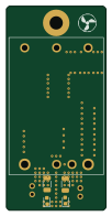
PCC
24 × 49 mm22 parts2LGPL-3.03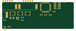 STM32
STM32Noggin g0b1ke
64.3 × 24 mm21 parts2LGPL-3.03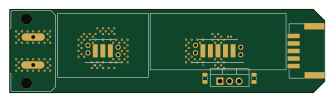
BackplaneTest
83.5 × 22 mm8 parts2LGPL-3.03
ESCB
36 × 18 mm8 parts2LGPL-3.03
Similar boards

Stack chan
stack-chan
50 × 50 mm33 parts2LApache-2.01.7k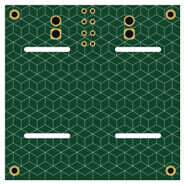
Cube batteryboard
willem-pennings
95 × 95 mm4 parts2LGPL-3.01.1k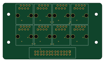
Mesabob
rene-dev
87.5 × 50 mm44 parts2LGPL-3.0979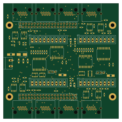
Bob
100 × 100 mm140 parts2LGPL-3.0979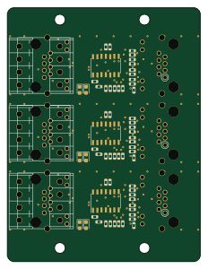
Triple adapter
57 × 75 mm26 parts2LGPL-3.0979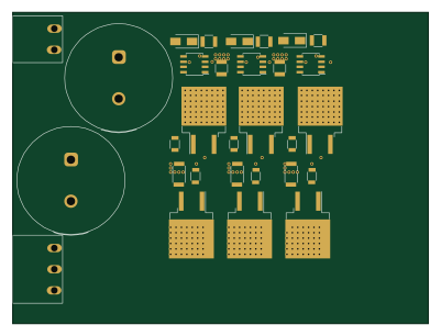
Trollerv2
100 × 75 mm33 parts4LGPL-3.0979