
Spi

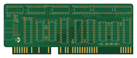
About the Spi PCB
Spi is an open source PCB design by scefrom, published on GitHub under the Custom license license. It is a 2-layer board measuring 135.9 × 53.3 mm, with 45 components from 23 distinct parts.
Other key parts include the 74HC125, 74HC164, 74HC04, 74HC153 and 74HC32. By type, the board carries 15 ICs, 9 resistors, 3 connectors, 3 diodes and 2 capacitors.
It belongs with the retro computing designs in this gallery.
From the project
A board featuring the Motorola 68000
Main components on the Spi
Spi bill of materials (BOM)
45 components, 23 distinct parts.
| Qty | Part | Footprint | Refs |
|---|---|---|---|
| 2 | 74HC125 | DIP-14_W7.62mm | U1, U2 |
| 1 | 74HC164 | DIP-14_W7.62mm | U3 |
| 1 | 74HC04 | DIP-14_W7.62mm | U4 |
| 1 | 74HC153 | DIP-16_W7.62mm | U5 |
| 1 | 74HC32 | DIP-14_W7.62mm | U6 |
| 3 | 74HC541 | DIP-20_W7.62mm | U7, U8, U10 |
| 1 | 74HC573 | DIP-20_W7.62mm | U9 |
| 1 | 74HC688 | DIP-20_W7.62mm | U11 |
| 1 | 74HC157 | DIP-16_W7.62mm | U12 |
| 1 | 74HC165 | DIP-16_W7.62mm | U13 |
| 2 | 74HC161 | DIP-16_W7.62mm | U14, U15 |
| 1 | spi-port | IDC-Header_2x05_P2.54mm_Horizontal | J1 |
| 1 | perslot1b | edge_connector_15p_2.54mm | J2 |
| 1 | perslot1a | edge_connector_30p_2.54mm | J3 |
| 9 | 100n | C_Disc_D3.0mm_W1.6mm_P7.62mm | B1, B2, B3, B4, B5, B7, B8, B9 +1 |
| 3 | 100n | C_Disc_D3.0mm_W1.6mm_P2.54mm | B6, B11, B12 |
| 1 | 10u | CP_Radial_D5.0mm_P2.00mm | B13 |
| 3 | D_Schottky_Filled | D_DO-35_SOD27_P2.54mm_Vertical_AnodeUp | D1, D2, D3 |
| 2 | 22pF | C_Disc_D3.0mm_W1.6mm_P2.54mm | C1, C2 |
| 2 | 1k | R_Axial_DIN0207_L6.3mm_D2.5mm_P2.54mm_Vertical | R2, R6 |
Show 3 more
| Qty | Part | Footprint | Refs |
|---|---|---|---|
| 4 | 10k | R_Axial_DIN0207_L6.3mm_D2.5mm_P2.54mm_Vertical | R3, R10, R11, R12 |
| 2 | 4k7 | R_Axial_DIN0207_L6.3mm_D2.5mm_P2.54mm_Vertical | R5, R9 |
| 1 | 2k | R_Axial_DIN0207_L6.3mm_D2.5mm_P2.54mm_Vertical | R7 |
Spi design files
The KiCad project lives in the scefrom/SF68 repository on GitHub; these links point at the commit this page was built from.
- Layoutspi/spi.kicad_pcb
- Schematicspi/spi.kicad_sch
Spi: common questions
How big is the Spi PCB?
The Spi measures 135.9 × 53.3 mm, has 2 copper layers and is 1.6 mm thick.
How many components are on the Spi?
45 components, from 23 distinct parts. The full bill of materials is listed on this page.
Where can I download the Spi design files?
From the scefrom/SF68 repository on GitHub, which has the KiCad layout and the schematic; the links under Design files point to each one.
Can I use the Spi design in my own project?
It is published under Custom license, which limits how it may be reused; read the license before building on it.
More boards in SF68
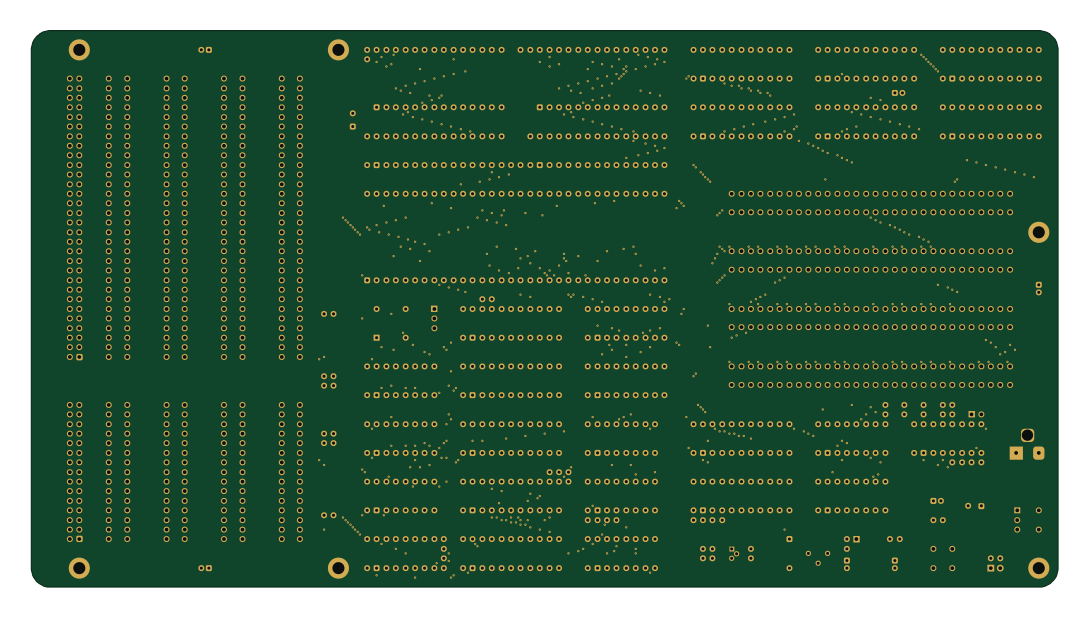
SF68
271.8 × 147.3 mm122 parts4LCustom license2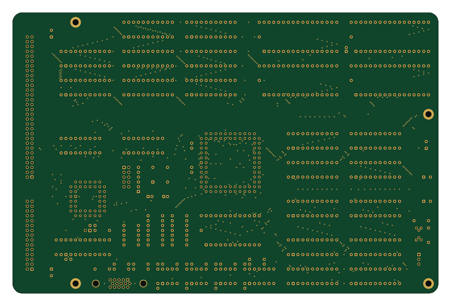
Vga cpld jtag
223.5 × 147.3 mm122 parts2LCustom license2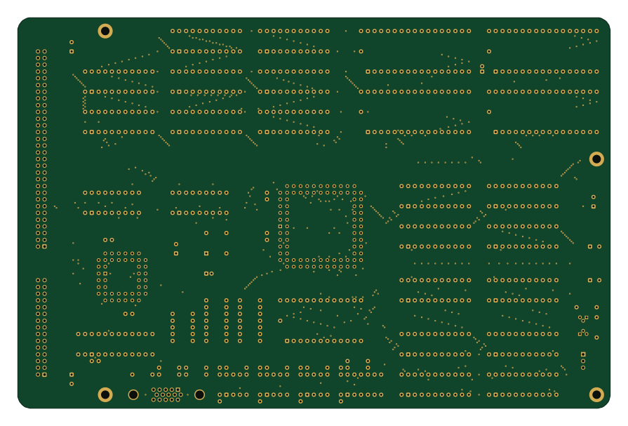
Vga cpld
223.5 × 147.3 mm116 parts2LCustom license2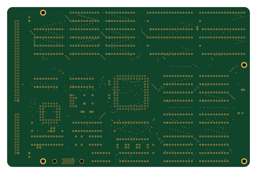
Vga cpld jtag fctlines
223.5 × 147.3 mm99 parts2LCustom license2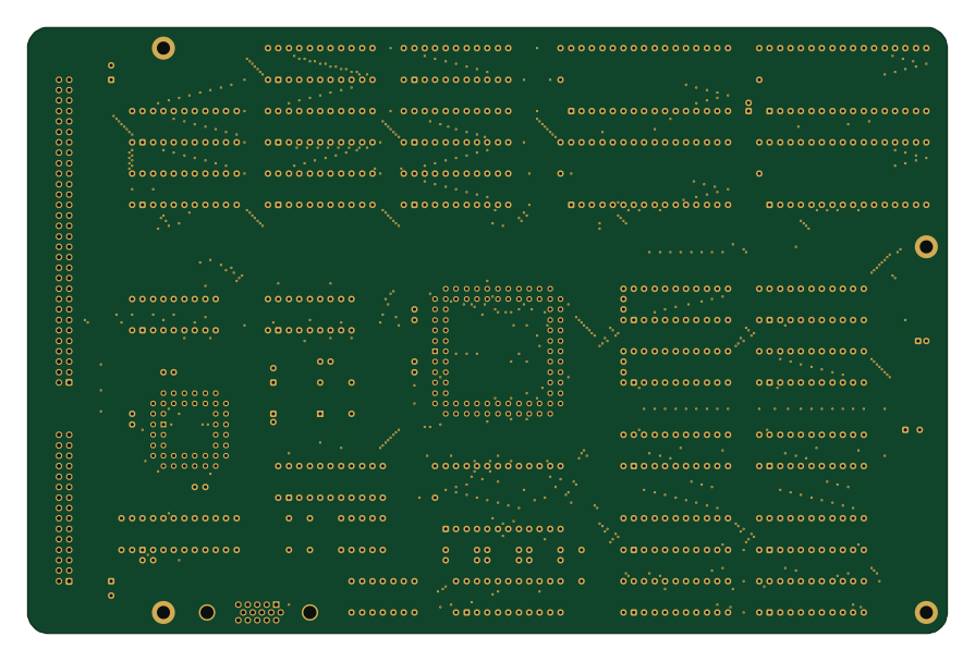
Vga cpld fctlines
223.5 × 147.3 mm99 parts2LCustom license2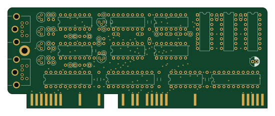
Ps2
137.2 × 53.3 mm58 parts2LCustom license2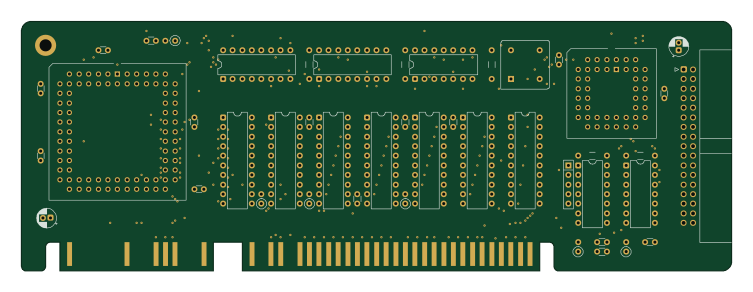
Floppy
188 × 66 mm33 parts2LCustom license2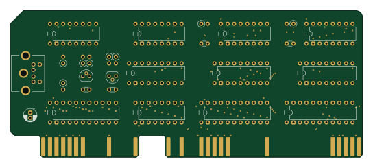
Ps2 old
135.9 × 56.5 mm29 parts2LCustom license2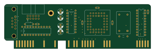
Uart
135.9 × 41.3 mm16 parts2LCustom license2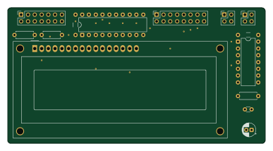
Lcd2x16
96.5 × 50.8 mm14 parts2LCustom license2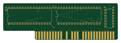
Ram1M
105.4 × 33.7 mm5 parts2LCustom license2
Similar boards
Expansion Card Retrofit
FrameworkComputer
24 × 27.3 mm5 parts2LCC-BY-4.01.1k
Rgb to hdmi
hoglet67
77 × 97 mm67 parts2LGPL-3.01.0k
Buffer
53.9 × 23.2 mm13 parts2LGPL-3.01.0k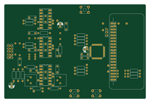
X1
121.9 × 81.3 mm51 parts2LGPL-3.01.0k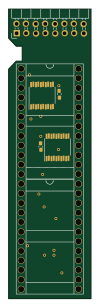
Amiga External
21.9 × 76.7 mm6 parts2LGPL-3.01.0k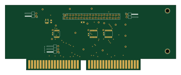
Videoslotadapter
152 × 57.6 mm13 parts2LGPL-3.01.0k