
ZAK181

About the ZAK181 PCB
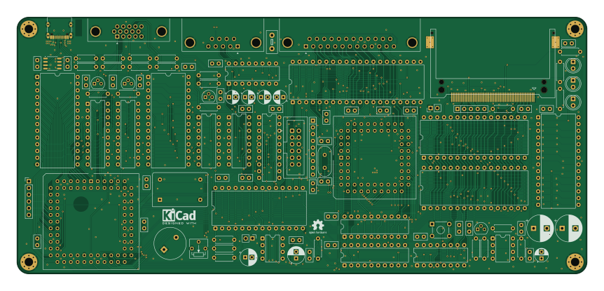
ZAK181 is an open source PCB design by agkaminski, published on GitHub under the CC-BY-NC-4.0 license. It is a 4-layer board measuring 215.3 × 96.8 mm, with 111 components from 55 distinct parts.
Other key parts include the Z8S18033VSG, Z80 PIO A, AY-3-8912, 74HC138 and LM386. By type, the board carries 43 capacitors, 27 resistors, 21 ICs, 6 connectors, 4 transistors and 3 diodes.
It belongs with the retro computing and keyboards designs in this gallery.
From the project
Improved ZAK180: DIY all-in-keyboard computer featuring Z180 and floppy drive.
- Z180 CPU, - 1 MB of static RAM, - 16 KB bootloader ROM, - Comact Flash slot in True IDE mode, - 16 bit GPIO user port, - 2 UARTs: USB-C and RS232, - AY-3-8912 sound, - 80x60 8-color text mode VGA output, - custom Cherry-MX mechanical keyboard, - USB-C powered.
Collection of useful datasheets, might be removed in the future.
Subrepository that contains a hardware project of a mechanical keyboard for the computer.
Main components on the ZAK181
ZAK181 bill of materials (BOM)
111 components, 55 distinct parts — part numbers from the project's BOM.
| Qty | Part | Footprint | Refs |
|---|---|---|---|
| 1 | Z8S18033VSG Z180 | PLCC-68_THT-Socket | IC1 |
| 1 | Z80 PIO A | DIP-40_W15.24mm | U2 |
| 1 | AY-3-8912 | DIP-28_W15.24mm | U3 |
| 1 | 74HC138 | DIP-16_W7.62mm | U8 |
| 1 | LM386 | DIP-8_W7.62mm | U17 |
| 1 | NE555P | DIP-8_W7.62mm | U18 |
| 1 | XC95108PC84 | PLCC-84_THT-Socket | U20 |
| 2 | 74HC377 | DIP-20_W7.62mm | U21, U30 |
| 1 | 74HC244 | DIP-20_W7.62mm | U22 |
| 1 | 27C64 | DIP-28_W15.24mm | U23 |
| 1 | 74HC166 | DIP-16_W7.62mm | U24 |
| 1 | MAX232 | DIP-16_W7.62mm | U25 |
| 1 | CH340N | SOP-8_3.9x4.9mm_P1.27mm | U26 |
| 1 | 62256 | DIP-28_W15.24mm | U27 |
| 2 | AS6C4008 | DIP-32_W15.24mm | U28, U40 |
| 1 | 27C128 | DIP-28_W15.24mm | U29 |
| 1 | ZAK181MD (GAL16V8) | DIP-20_W7.62mm | U31 |
| 1 | 74HC157 | DIP-16_W7.62mm | U32 |
| 1 | ZAK181AY (GAL16V8) | DIP-20_W7.62mm | U33 |
| 4 | BC547 | TO-92 | Q2, Q3, Q4, Q5 |
Show 35 more
| Qty | Part | Footprint | Refs |
|---|---|---|---|
| 1 | 25.175 MHz | Oscillator_DIP-14 | X1 |
| 1 | 12.288 MHz | Crystal_HC49-4H_Vertical | Y2 |
| 1 | JTAG | PinHeader_1x06_P2.54mm_Vertical | J1 |
| 1 | Compact Flash | Conn_CF_N7E50-Q516XX-40 | J3 |
| 1 | Speaker | PinHeader_1x02_P2.54mm_Vertical | J4 |
| 1 | Keyboard | IDC-Header_2x06_P2.54mm_Vertical | J5 |
| 1 | USB C | USB_C_Receptacle_G-Switch_GT-USB-7010ASV | J8 |
| 1 | Reset | PinHeader_1x02_P2.54mm_Vertical | J9 |
| 1 | Fuse | Fuse_Littelfuse_395Series | F1 |
| 1 | JUMPER_2_BRIDGED Jumper_2_Bridged | SolderJumper-2_P1.3mm_Bridged_Pad1.0x1.5mm | JP1 |
| 1 | Speaker | MagneticBuzzer_StarMicronics_QMB-105 | LS1 |
| 1 | 1K | Potentiometer_Vishay_T73YP_Vertical | RV1 |
| 1 | Reset | SW_TH_Tactile_Omron_B3F-10xx | SW1 |
| 1 | HALT | LED_D5.0mm | D1 |
| 1 | POWER | LED_D5.0mm | D2 |
| 1 | ACTIVITY | LED_D5.0mm | D3 |
| 29 | 100N 100n | C_Disc_D5.0mm_W2.5mm_P2.50mm | C4, C5, C6, C7, C8, C9, C10, C11 +21 |
| 1 | 47N 47n | C_Disc_D5.0mm_W2.5mm_P2.50mm | C27 |
| 2 | 150U 150u | CP_Radial_D6.3mm_P2.50mm | C28, C29 |
| 5 | 10U 10u | CP_Radial_D5.0mm_P2.50mm | C30, C49, C50, C51, C58 |
| 1 | 10N 10n | C_Disc_D5.0mm_W2.5mm_P2.50mm | C33 |
| 2 | 22P 22p | C_Disc_D5.0mm_W2.5mm_P2.50mm | C38, C39 |
| 2 | 470U 470u | CP_Radial_D10.0mm_P5.00mm | C54, C55 |
| 1 | 100P 100p | C_Disc_D5.0mm_W2.5mm_P2.50mm | C73 |
| 3 | 390R | R_Axial_DIN0207_L6.3mm_D2.5mm_P7.62mm_Horizontal | R6, R11, R14 |
| 6 | 3K3 | R_Axial_DIN0207_L6.3mm_D2.5mm_P7.62mm_Horizontal | R7, R8, R9, R10, R12, R13 |
| 3 | 100R | R_Axial_DIN0207_L6.3mm_D2.5mm_P7.62mm_Horizontal | R15, R16, R20 |
| 4 | 1K | R_Axial_DIN0207_L6.3mm_D2.5mm_P7.62mm_Horizontal | R19, R33, R38, R39 |
| 3 | 2K2 | R_Axial_DIN0207_L6.3mm_D2.5mm_P7.62mm_Horizontal | R26, R27, R28 |
| 1 | 10R | R_Axial_DIN0207_L6.3mm_D2.5mm_P7.62mm_Horizontal | R29 |
| 2 | 10K | R_Axial_DIN0207_L6.3mm_D2.5mm_P7.62mm_Horizontal | R30, R32 |
| 1 | 220K | R_Axial_DIN0207_L6.3mm_D2.5mm_P7.62mm_Horizontal | R31 |
| 2 | 5K6 | R_Axial_DIN0207_L6.3mm_D2.5mm_P7.62mm_Horizontal | R34, R35 |
| 1 | 47K | R_Array_SIP9 | RN2 |
| 1 | 1K | R_Array_SIP5 | RN3 |
ZAK181 design files
The KiCad project lives in the agkaminski/ZAK181 repository on GitHub; these links point at the commit this page was built from.
- Layoutkicad/zak181.kicad_pcb
- Schematickicad/zak181.kicad_sch
- BOMkicad/production/bom.csv
ZAK181: common questions
How big is the ZAK181 PCB?
The ZAK181 measures 215.3 × 96.8 mm, has 4 copper layers and is 1.6 mm thick.
How many components are on the ZAK181?
111 components, from 55 distinct parts, with part numbers taken from the project's own BOM. The full bill of materials is listed on this page.
Where can I download the ZAK181 design files?
From the agkaminski/ZAK181 repository on GitHub, which has the KiCad layout, the schematic and the BOM; the links under Design files point to each one.
Can I use the ZAK181 design in my own project?
It is published under CC-BY-NC-4.0, which limits how it may be reused; read the license before building on it.
More boards in ZAK181
Similar boards
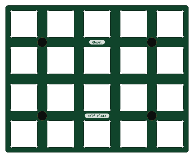
Half plate
tzarc
95.3 × 76.2 mm24 parts2LCERN-OHL-S-2.0988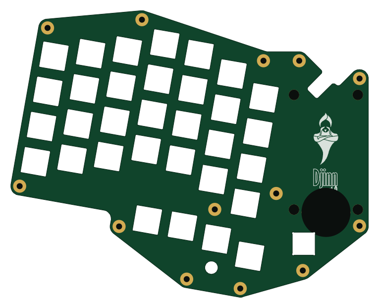
Board-DjinnPlate
191 × 152.9 mm4 parts2LCERN-OHL-S-2.0988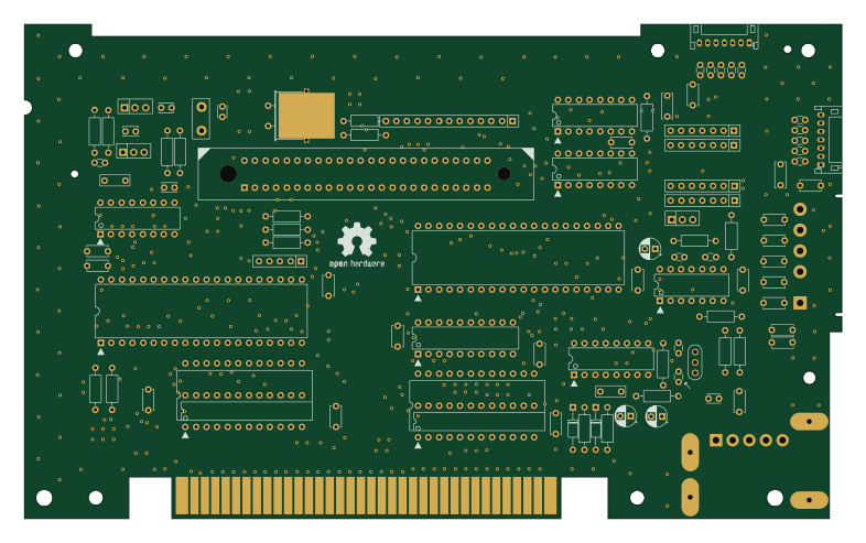
OpenTendo
Redherring32
196.3 × 118.7 mm93 parts2LTAPR-OHL-1.0850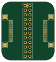
24pin flex interposer
Wren6991
29 × 32 mm3 parts2LNo license508
Sram dev board
50 × 50 mm12 parts2LNo license508
GB-BRK-SLOT-A
Gekkio
81 × 80 mm20 parts2LCC-BY-4.0376