
MegaBlaster2

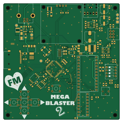
About the MegaBlaster2 PCB
MegaBlaster2 is an open source Microchip SAM PCB design by AidanHockey5, published on GitHub under the AGPL-3.0 license. It is a 4-layer board measuring 99 × 99 mm, with 102 components from 46 distinct parts.
Its main chip is the ATSAMD51J19A-A, from the Microchip SAM family. Other key parts include the LM2733XMF, LD1117S33TR_SOT223, LD1117S50TR_SOT223, W25Q32JVSS and Si5351A-B-GT. By type, the board carries 42 capacitors, 29 resistors, 11 ICs, 7 switches, 4 connectors and 3 inductors.
It belongs with the retro computing designs in this gallery.
From the project
The latest iteration of my hardware Sega Genesis/Megadrive Video Game Music Player
Demo video can be found here: https://www.youtube.com/watch?v=4sKwGWfikdc
This project contains the source material for the Mega Blaster 2, a hardware Sega Genesis/Mega Drive video game music (VGM) player that utilizes the real sound chips. Play any Genesis track on-demand with brilliant sound quality on the actual YM2612/YM3438 and SN76489 PSG synthesizer chips that were found in the real Genesis consoles(1). The Mega Blaster 2 is compatible with both .vgm and .vgz files and can support both the YM2612 and YM3438 simply by changing the DIP switch values. This unit does not use any emulated…
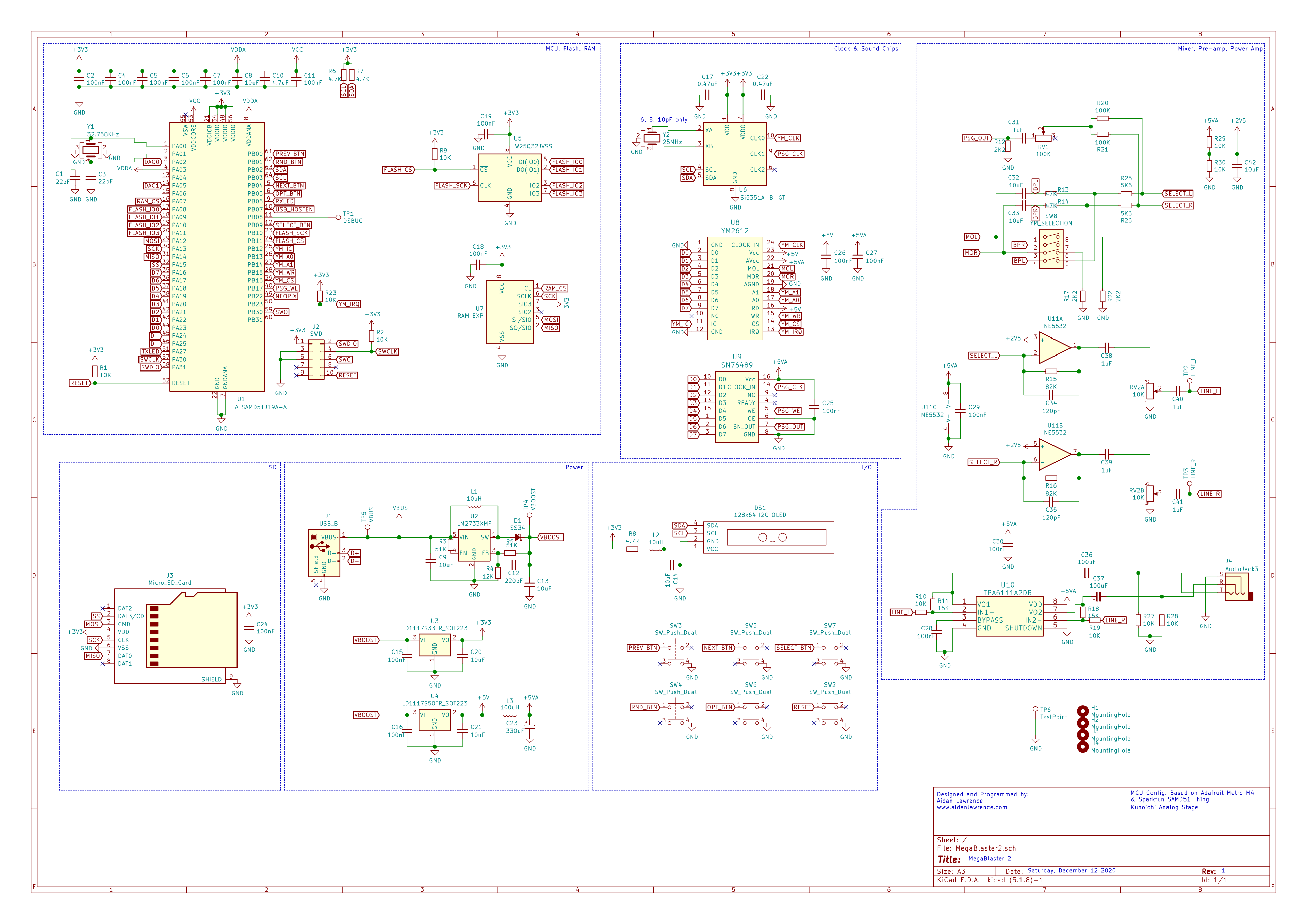
Main components on the MegaBlaster2
MegaBlaster2 bill of materials (BOM)
102 components, 46 distinct parts.
| Qty | Part | Footprint | Refs |
|---|---|---|---|
| 1 | ATSAMD51J19A-A | TQFP-64_10x10mm_P0.5mm | U1 |
| 1 | LM2733XMF | SOT-23-5 | U2 |
| 1 | LD1117S33TR_SOT223 | SOT-223-3_TabPin2 | U3 |
| 1 | LD1117S50TR_SOT223 | SOT-223-3_TabPin2 | U4 |
| 1 | W25Q32JVSS | SOIC-8_5.23x5.23mm_P1.27mm | U5 |
| 1 | Si5351A-B-GT | MSOP-10_3x3mm_P0.5mm | U6 |
| 1 | RAM_EXP | SOIC-8_3.9x4.9mm_P1.27mm | U7 |
| 1 | YM2612 | DIP-24_W15.24mm_Socket | U8 |
| 1 | SN76489 | DIP-16_W7.62mm_Socket | U9 |
| 1 | TPA6111A2DR | SOIC-8_3.9x4.9mm_P1.27mm | U10 |
| 1 | NE5532 | SOIC-8_3.9x4.9mm_P1.27mm | U11 |
| 1 | 32.768KHz | Crystal_SMD_SeikoEpson_MC306-4Pin_8.0x3.2mm | Y1 |
| 1 | 25MHz | Crystal_SMD_3225-4Pin_3.2x2.5mm | Y2 |
| 1 | USB_B | USB_B_Lumberg_2411_02_Horizontal | J1 |
| 1 | SWD | PinHeader_2x05_P1.27mm_Vertical | J2 |
| 1 | Micro_SD_Card | SOFNG_TF_15x15_PUSH_PUSH | J3 |
| 1 | AudioJack3 | SWITCHCRAFT_35RAPC4BHN2 | J4 |
| 1 | 100K | 3362P-1-103LF | RV1 |
| 1 | 10K | Potentiometer_Alps_RK097_Dual_Horizontal | RV2 |
| 6 | SW_Push_Dual | SW_TH_Tactile_Omron_B3F-10xx | SW2, SW3, SW4, SW5, SW6, SW7 |
Show 26 more
| Qty | Part | Footprint | Refs |
|---|---|---|---|
| 1 | YM_SELECTION | SW_DIP_SPSTx04_Slide_9.78x12.34mm_W7.62mm_P2.54mm | SW8 |
| 1 | 128x64_I2C_OLED | oled_128x64 | DS1 |
| 1 | SS34 | D_SMA | D1 |
| 2 | 10uH | L_4x4 | L1, L2 |
| 1 | 100uH | 6x6Inductor | L3 |
| 2 | 22pF | C_0603_1608Metric | C1, C3 |
| 17 | 100nF | C_0805_2012Metric | C2, C4, C5, C6, C7, C11, C15, C16 +9 |
| 9 | 10uF | C_1206_3216Metric | C8, C9, C13, C14, C20, C21, C32, C33 +1 |
| 1 | 4.7uF | C_0805_2012Metric | C10 |
| 1 | 220pF | C_0603_1608Metric | C12 |
| 2 | 0.47uF | C_0805_2012Metric | C17, C22 |
| 1 | 330uF | CP_Elec_8x10 | C23 |
| 5 | 1uF | C_0805_2012Metric | C31, C38, C39, C40, C41 |
| 2 | 120pF | C_0603_1608Metric | C34, C35 |
| 2 | 100uF | CP_Elec_6.3x7.7 | C36, C37 |
| 10 | 10K | R_0805_2012Metric | R1, R2, R9, R10, R19, R23, R27, R28 +2 |
| 2 | 51K | R_0805_2012Metric | R3, R5 |
| 1 | 12K | R_0805_2012Metric | R4 |
| 2 | 4.7K | R_0805_2012Metric | R6, R7 |
| 1 | 4.7R | R_0805_2012Metric | R8 |
| 2 | 15K | R_0805_2012Metric | R11, R18 |
| 3 | 2K2 | R_0805_2012Metric | R12, R17, R22 |
| 2 | 47K | R_0805_2012Metric | R13, R14 |
| 2 | 82K | R_0805_2012Metric | R15, R16 |
| 2 | 100K | R_0805_2012Metric | R20, R21 |
| 2 | 5K6 | R_0805_2012Metric | R25, R26 |
MegaBlaster2 design files
The KiCad project lives in the AidanHockey5/MegaBlaster2 repository on GitHub; these links point at the commit this page was built from.
MegaBlaster2: common questions
What microcontroller does the MegaBlaster2 use?
The MegaBlaster2 is built around the ATSAMD51J19A-A, from the Microchip SAM family.
How big is the MegaBlaster2 PCB?
The MegaBlaster2 measures 99 × 99 mm, has 4 copper layers and is 1.6 mm thick.
How many components are on the MegaBlaster2?
102 components, from 46 distinct parts. The full bill of materials is listed on this page.
Where can I download the MegaBlaster2 design files?
From the AidanHockey5/MegaBlaster2 repository on GitHub, which has the KiCad layout; the links under Design files point to each one.
Can I use the MegaBlaster2 design in my own project?
Yes, under the terms of its AGPL-3.0 license, which AidanHockey5 chose for the repository.
Can I test firmware for the MegaBlaster2 without the hardware?
Yes. HardLabs builds a simulation of the board from its netlist and BOM, so you can run and debug Microchip SAM firmware against it before you order a PCB.
Similar boards
 Microchip SAM
Fpgaboy
Wren6991
50 × 50 mm89 parts4LNo license508 Microchip SAM
Kira
kiibohd
366.9 × 114.3 mm400 partsCERN-OHL-1.2415 Microchip SAM
DSKY driver
benkrasnow
43 × 92.3 mm44 partsMIT258 Microchip SAM
Duet 2 Maestro
Duet3D
100 × 123 mm336 partsCERN-OHL-1.2257 Microchip SAM
Makennbot
idlehandsdev
60 × 75 mm53 parts2LNo license175 Microchip SAM
Oxidized flash
blakesmith
61 × 21.6 mm19 parts2LNo license167