
Anice

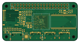
About the Anice PCB
Anice is an open source FPGA PCB design by hackclub, published on GitHub. It is a 4-layer board measuring 65.6 × 34 mm, with 91 components from 36 distinct parts.
Its main chip is the ECP5U_12_CABGA256, from the FPGA family. Other key parts include the TPD2EUSB30, FT231XQ, PCA9306DC1, W9825G6KH-6 and W25Q128JVS. By type, the board carries 38 capacitors, 25 resistors, 11 ICs, 6 connectors, 3 inductors and 1 crystal.
From the project
A YSWS for the northern hemisphere's summer and the aussie's winter. Run by @pmnlla, with love and loads of carrots.
"FPGAs work like this. You don't tell them what to do, you tell them what to BE."
An FPGA is a chip that can be configured on the hardware level. You can basically make your own CPU and GPU on it.
The PCB called is "anice": - 256MiB of ram - 128MiB of flash - HDMI port - triple USB C with JTAG converter - SDCard Reader - dual 25MHz clock and 200MHz built-in clock - multiple indicator lights - only 4 layer PCB

Main components on the Anice
Anice bill of materials (BOM)
91 components, 36 distinct parts — part numbers from the project's BOM.
| Qty | Part | Footprint | Refs |
|---|---|---|---|
| 1 | ECP5U_12_CABGA256 | BGA-256_14.0x14.0mm_Layout16x16_P0.8mm_Ball0.45mm_Pad0.32mm_NSMD | U1 |
| 3 | TPD2EUSB30 | Texas_DRT-3 | U5, U6, U8 |
| 1 | FT231XQ | QFN-20-1EP_4x4mm_P0.5mm_EP2.5x2.5mm | U7 |
| 1 | PCA9306DC1 | VSSOP-8_2.3x2mm_P0.5mm | U9 |
| 1 | W9825G6KH-6 | TSOP-II-54_22.2x10.16mm_P0.8mm | U10 |
| 1 | W25Q128JVS | SOIC-8_5.3x5.3mm_P1.27mm | U11 |
| 3 | TLV62569DRL | SOT-563 | U12, U13, U14 |
| 1 | ECS-2520MV-XXX-XX ECS-2520MV-xxx-xx | Crystal_SMD_3225-4Pin_3.2x2.5mm | Y1 |
| 1 | CONN_02X20_COUNTER_CLOCKWISE Conn_02x20_Counter_Clockwise | PinHeader_2x20_P2.54mm_Vertical | J1 |
| 1 | MICRO_SD_CARD_DET1 Micro_SD_Card_Det1 | SDCard molex | J2 |
| 3 | USB_C_RECEPTACLE_USB2.0_14P USB_C_Receptacle_USB2.0_14P | USB_C_Receptacle_GCT_USB4105-xx-A_16P_TopMnt_Horizontal | J3, J4, J5 |
| 1 | HDMI_C_1.3 | XKB Connection A71-05H4-111N1 | J7 |
| 3 | 15K 15k | R_0603_1608Metric | RA1, RA2, RA3 |
| 1 | 18K 18k | R_0603_1608Metric | RB1 |
| 1 | 4.7K 4.7k | R_0603_1608Metric | RB2 |
| 1 | 3.3K 3.3k | R_0603_1608Metric | RB3 |
| 1 | RED | LED_0603_1608Metric | D1 |
| 3 | 2.2UH 2.2uH | L_1008_2520Metric | L1, L2, L3 |
| 11 | 10UF 10uF | C_0603_1608Metric | C2, C3, C4, C8, C9, C11, C12, C25 +3 |
| 4 | 100PF 100pF | C_0603_1608Metric | C10, C21, C27, C29 |
Show 16 more
| Qty | Part | Footprint | Refs |
|---|---|---|---|
| 8 | 22NF 22nF | C_0603_1608Metric | C13, C14, C15, C16, C17, C18, C19, C20 |
| 1 | CC0805ZKY5V5BB226 22uF | C_0603_1608Metric | C22 |
| 13 | 100NF 100nF | C_0402_1005Metric | C23, C26, C31, C33, C34, C35, C36, C37 +5 |
| 1 | 15PF 15pF | C_0402_1005Metric | C40 |
| 6 | 5.1K 5.1k | R_0603_1608Metric | R1, R2, R3, R4, R6, R7 |
| 1 | 549 | R_0603_1608Metric | R5 |
| 2 | 470 | R_0603_1608Metric | R8, R10 |
| 4 | 10K 10k | R_0603_1608Metric | R9, R20, R21, R22 |
| 1 | 100K 100k | R_0603_1608Metric | R11 |
| 2 | 4.7K 4.7k | R_0603_1608Metric | R12, R13 |
| 2 | 3.3K 3.3k | R_0603_1608Metric | R14, R15 |
| 3 | AC0603FR-104K7L 4.7k | R_0603_1608Metric | R16, R17, R24 |
| 1 | 1k | R_0603_1608Metric | R18 |
| 1 | RC0603FR-0710KL 10k | R_0603_1608Metric | R19 |
| 1 | RC0402JR-075K1Ln 4.7k Yageo | R_0603_1608Metric | R23 |
| 1 | 73L2R47J 0.47 | R_0603_1608Metric | R38 |
Anice design files
The KiCad project lives in the hackclub/reflow repository on GitHub; these links point at the commit this page was built from.
Anice: common questions
What microcontroller does the Anice use?
The Anice is built around the ECP5U_12_CABGA256, from the FPGA family.
How big is the Anice PCB?
The Anice measures 65.6 × 34 mm, has 4 copper layers and is 1.6 mm thick.
How many components are on the Anice?
91 components, from 36 distinct parts, with part numbers taken from the project's own BOM. The full bill of materials is listed on this page.
Where can I download the Anice design files?
From the hackclub/reflow repository on GitHub, which has the KiCad layout, the schematic and the BOM; the links under Design files point to each one.
Can I use the Anice design in my own project?
The repository has no license, so all rights stay with hackclub. Use it as a reference, and ask the author before reusing the design.
Can I test firmware for the Anice without the hardware?
Yes. HardLabs builds a simulation of the board from its netlist and BOM, so you can run and debug FPGA firmware against it before you order a PCB.
More boards in reflow
 RP2040/RP2350
Usb charging hub
80 × 95 mm206 parts4LNo license2 RP2040/RP2350
Phase interferometer
54.3 × 76.1 mm78 parts4LNo license2 RP2040/RP2350
Badge
73 × 41 mm65 parts2LNo license2 AVR/Arduino
MP3 Player
52 × 43 mm42 parts2LNo license2
Reflow example
47 × 44 mm28 parts2LNo license2
Similar boards
 FPGA
FPGABase board
GlasgowEmbedded
80 × 49 mm222 parts4L0BSD2.2k FPGA
FPGAThunderscope Rev5.3
EEVengers
122.5 × 103.5 mm817 parts6LMIT1.3k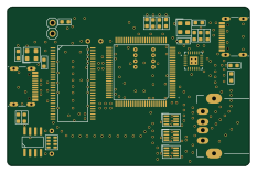 FPGA
FPGAUsb sniffer
ataradov
58.2 × 38.1 mm86 parts2LBSD-3-Clause1.3k FPGA
FPGATomu, I'm
theacodes
13 × 9.4 mm40 parts4LMIT1.1k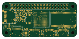 FPGA
FPGAIcepi zero
cheyao
65 × 30 mm143 parts4LSHL-2.1828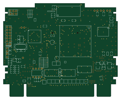 FPGA
FPGASd2snes
mrehkopf
101.5 × 83 mm147 partsGPL-2.0717