
S100 enet

About the S100 enet PCB
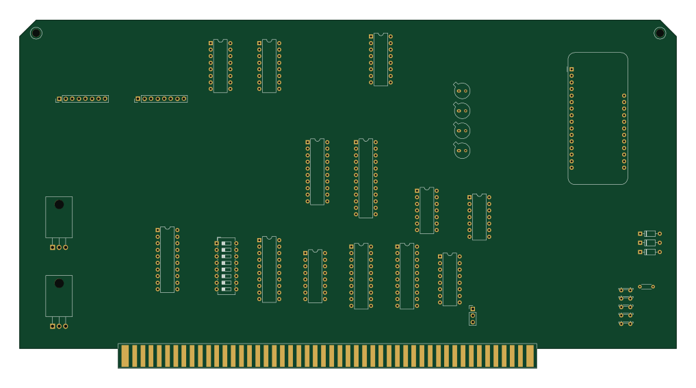
S100 enet is an open source PCB design by jayacotton, published on GitHub under the MIT license. It is a 2-layer board, with 34 components from 25 distinct parts.
Other key parts include the 74LS10, 74LS688, 74LS163, 74HC02 and L7805. By type, the board carries 15 ICs, 7 diodes, 6 resistors, 4 connectors, 1 module and 1 switch.
It belongs with the retro computing designs in this gallery.
From the project
Inet tools for z80-rc2014 tcp/ip stack code.
In this section we have the BOM for the MT011 board as built for my needs.
For the best and current information about the MT011 board see https://github.com/markt4311/MT011.git
Find here the mt011-bom.ods a spread sheet for the BOM of the board. And the schematic (copied from above) MT011SPIWIZNET.pdf
I will include a picture of the board as built.
This board is now working on 18mhz cpu rc2014 systems.
Main components on the S100 enet
S100 enet bill of materials (BOM)
34 components, 25 distinct parts.
| Qty | Part | Footprint | Refs |
|---|---|---|---|
| 1 | 74LS10 | U1 | |
| 1 | 74LS688 | U2 | |
| 1 | 74LS163 | U3 | |
| 1 | 74HC02 | U4 | |
| 1 | L7805 | TO-220-3_Horizontal_TabDown | U5 |
| 1 | SPX2920U-3.3_TO220 | TO-220-3_Horizontal_TabDown | U6 |
| 1 | 74LS138 | U7 | |
| 1 | 74LS595 | U8 | |
| 1 | 74LS175 | U9 | |
| 1 | 22V10 | U10 | |
| 1 | 74LS165 | U11 | |
| 3 | 74LS245 | U12, U14, U15 | |
| 1 | 74LS245 | DIP-20_W7.62mm_Socket | U13 |
| 1 | Adafruit FeatherWing Ethernet board PN 3201 | LQFP-48_7x7mm_P0.5mm | A1 |
| 1 | FRAM socket | J1 | |
| 1 | SD Socket | Harwin_M20-89008xx_1x08_P2.54mm_Horizontal | J2 |
| 1 | ClockSelect | PinHeader_1x03_P2.54mm_Vertical | J3 |
| 1 | S100_MALE | S100_MALE | P1 |
| 1 | SW_DIP_x08 | SW1 | |
| 3 | 1N4148 | D_DO-35_SOD27_P7.62mm_Horizontal | D1, D2, D3 |
Show 5 more
| Qty | Part | Footprint | Refs |
|---|---|---|---|
| 3 | yellow | TO-18-2_Window | D4, D5, D6 |
| 1 | red | TO-18-2_Window | D7 |
| 1 | 20K | R_LDR_5.2x5.2mm_P3.5mm_Horizontal | R1 |
| 1 | 4.7K | R2 | |
| 4 | 470 | R_LDR_5.2x5.2mm_P3.5mm_Horizontal | R3, R4, R5, R6 |
S100 enet design files
The KiCad project lives in the jayacotton/inettools-z80 repository on GitHub; these links point at the commit this page was built from.
- Layoutboard/s100_enet.kicad_pcb
- Schematicboard/s100_enet.kicad_sch
S100 enet: common questions
How big is the S100 enet PCB?
The S100 enet has 2 copper layers and is 1.6 mm thick.
How many components are on the S100 enet?
34 components, from 25 distinct parts. The full bill of materials is listed on this page.
Where can I download the S100 enet design files?
From the jayacotton/inettools-z80 repository on GitHub, which has the KiCad layout and the schematic; the links under Design files point to each one.
Can I use the S100 enet design in my own project?
Yes, under the terms of its MIT license, which jayacotton chose for the repository.
More boards in inettools-z80
Similar boards
OpenTendo
Redherring32
196.3 × 118.7 mm93 parts2LTAPR-OHL-1.0850
MCL86jr
MicroCoreLabs
56.1 × 57.1 mm66 parts4LNo license532
24pin flex interposer
Wren6991
29 × 32 mm3 parts2LNo license508
Sram dev board
50 × 50 mm12 parts2LNo license508
TRS-80 Color Computer 3
baldengineer
280 × 155.3 mm204 parts2LCC-BY-4.0442
Commodore Plus 4
284.7 × 158.9 mm212 parts2LCC-BY-4.0442