
RC107-68000 ROM RAM 1

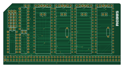
About the RC107-68000 ROM RAM 1 PCB
RC107-68000 ROM RAM 1 is an open source PCB design by MarkD833, published on GitHub under the CC-BY-NC-4.0 license. It is a 4-layer board measuring 101.6 × 53.3 mm, with 28 components from 10 distinct parts.
Other key parts include the 74LS125, 74LS139, SST39SF040, 74LS138 and AS6C4008-55PCN. By type, the board carries 12 connectors, 7 ICs, 7 capacitors and 2 resistors.
It belongs with the retro computing designs in this gallery.
From the project
My Motorola 68000 & 68302 processors (+ SIO, PIO & MFP boards) for the RCBus ecosystem.
Note: If this is the only memory board in the 68000 system, then a pair of FLASH chips should be assigned to /CS0 so that the 68000 finds the stack pointer and program counter on boot.
Note: If this board is used with an MC68302 processor, then see the note further down regarding the ability to remap the ROM & RAM devices.
Note the location of the decoupling capacitors for the memory devices are located within the IC sockets. THese decoupling capacitors should be bent over so that they do not interfere with the insertion of the memory chips.
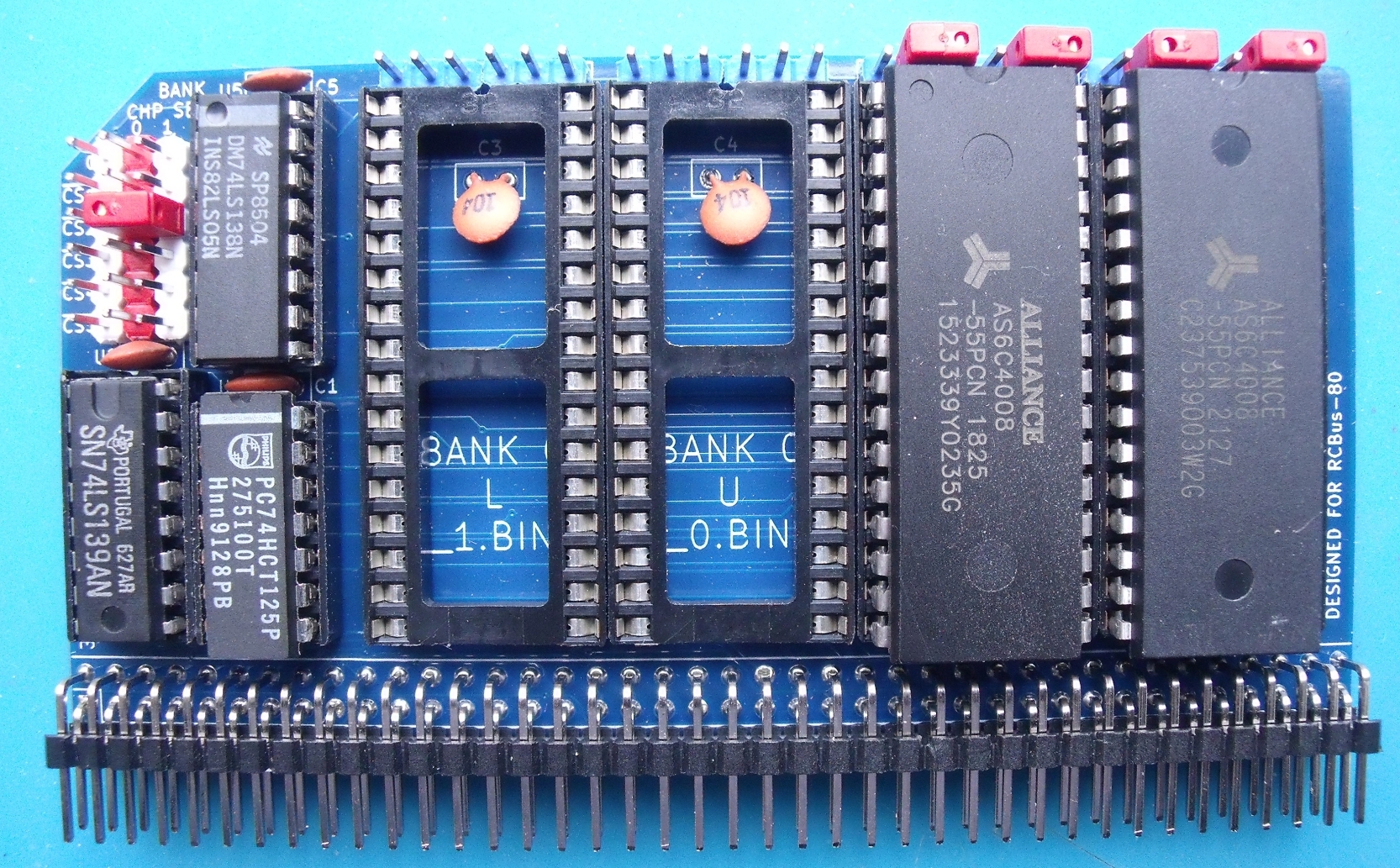
Main components on the RC107-68000 ROM RAM 1
RC107-68000 ROM RAM 1 bill of materials (BOM)
28 components, 10 distinct parts — part numbers from the project's BOM.
| Qty | Part | Footprint | Refs |
|---|---|---|---|
| 1 | 74LS125 | DIP-14_W7.62mm | U1 |
| 1 | 74LS139 | DIP-16_W7.62mm | U2 |
| 2 | SST39SF040 | DIP-32_W15.24mm | U3, U4 |
| 1 | 74LS138 | DIP-16_W7.62mm | U5 |
| 2 | AS6C4008-55PCN | DIP-32_W15.24mm | U6, U7 |
| 1 | RCBUS_80PIN_68000 RCBus_80PIN_68000 | RCBus_80p_Medium | J1 |
| 8 | CONN_01X03 Conn_01x03 | PinHeader_1x03_P2.54mm_Vertical | J2, J3, J4, J5, J6, J7, J8, J9 |
| 3 | CONN_01X06 Conn_01x06 | PinHeader_1x06_P2.54mm_Vertical | J10, J11, J12 |
| 7 | 100N 100n | C_Disc_D5.0mm_W2.5mm_P2.50mm | C1, C2, C3, C4, C5, C6, C7 |
| 2 | 10K | R_Axial_DIN0207_L6.3mm_D2.5mm_P7.62mm_Horizontal | R1, R2 |
RC107-68000 ROM RAM 1 design files
The KiCad project lives in the MarkD833/RCBUS-68xxx repository on GitHub; these links point at the commit this page was built from.
RC107-68000 ROM RAM 1: common questions
How big is the RC107-68000 ROM RAM 1 PCB?
The RC107-68000 ROM RAM 1 measures 101.6 × 53.3 mm, has 4 copper layers and is 1.6 mm thick.
How many components are on the RC107-68000 ROM RAM 1?
28 components, from 10 distinct parts, with part numbers taken from the project's own BOM. The full bill of materials is listed on this page.
Where can I download the RC107-68000 ROM RAM 1 design files?
From the MarkD833/RCBUS-68xxx repository on GitHub, which has the KiCad layout, the schematic and the BOM; the links under Design files point to each one.
Can I use the RC107-68000 ROM RAM 1 design in my own project?
It is published under CC-BY-NC-4.0, which limits how it may be reused; read the license before building on it.
More boards in RCBUS-68xxx
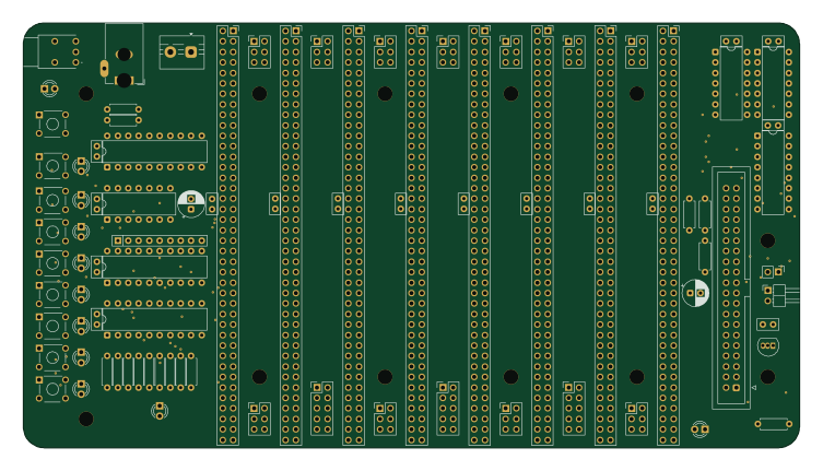
RC200-Dev Backplane
188 × 102.9 mm90 parts2LCC-BY-NC-4.08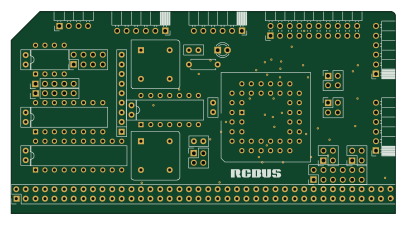
RC202-68000 SIO 1
101.6 × 53.3 mm40 parts4LCC-BY-NC-4.08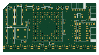
68302 CPU Board
101.6 × 53.3 mm37 parts4LCC-BY-NC-4.08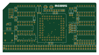
RC201-68000 CPU 2
101.6 × 53.3 mm37 parts4LCC-BY-NC-4.08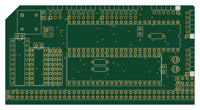
68000 LBE Board
101.6 × 53.3 mm34 parts4LCC-BY-NC-4.08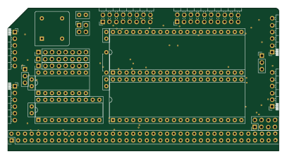
68000 SIO BOARD
101.6 × 53.3 mm33 parts4LCC-BY-NC-4.08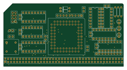
68000 CPU Board
101.6 × 53.3 mm32 parts4LCC-BY-NC-4.08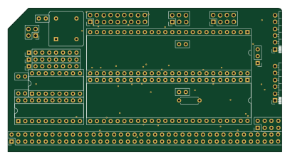
68000 MPF BOARD
101.6 × 53.3 mm27 parts4LCC-BY-NC-4.08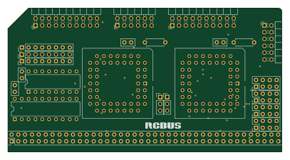
RC203-68000 PIO 1
101.6 × 53.3 mm24 parts4LCC-BY-NC-4.08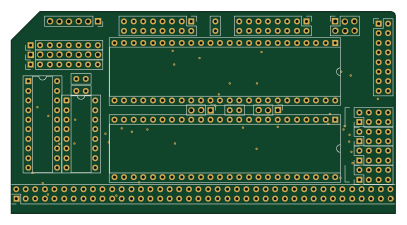
68000 PIO BOARD
101.6 × 53.3 mm23 parts4LCC-BY-NC-4.08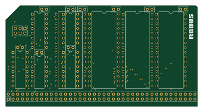
RC208-68000 BOOTROM RAM 2
101.6 × 53.3 mm20 parts4LCC-BY-NC-4.08
Similar boards
Amiga External
hoglet67
21.9 × 76.7 mm6 parts2LGPL-3.01.0k
Atari pickup
26.4 × 53.9 mm7 parts2LGPL-3.01.0k
Deniseadapter
26.7 × 62.2 mm16 parts2LGPL-3.01.0k
Analog
53.9 × 23.2 mm33 parts2LGPL-3.01.0k
Rgb to hdmi
77 × 97 mm67 parts2LGPL-3.01.0k
Buffer
53.9 × 23.2 mm13 parts2LGPL-3.01.0k