
Karabas go

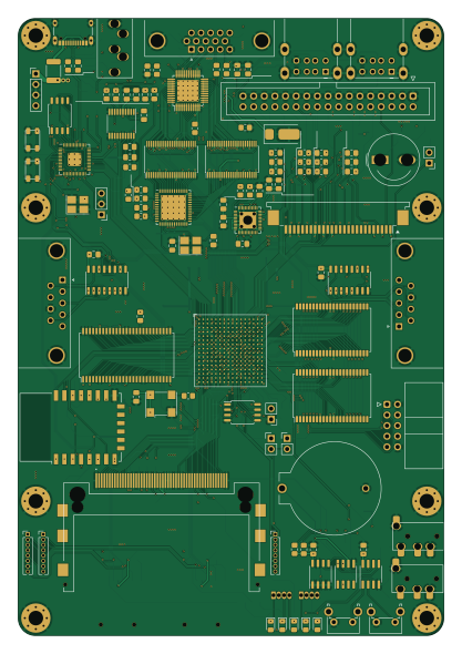
About the Karabas go PCB
Karabas go is an open source RP2040/RP2350 PCB design by andykarpov, published on GitHub under the CC-BY-NC-4.0 license. It is a 4-layer board measuring 101.6 × 147.3 mm, with 279 components from 100 distinct parts.
Its main chip is the RP2040, from the RP2040/RP2350 family. Other key parts include the XC6SLX25-FTG256, LM1117MP-3.3, W25Q128JVSIQ, PCA9536D and 74HC597. By type, the board carries 110 capacitors, 96 resistors, 30 ICs, 17 connectors, 8 diodes and 4 crystals.
From the project
Karabas-Go PCB
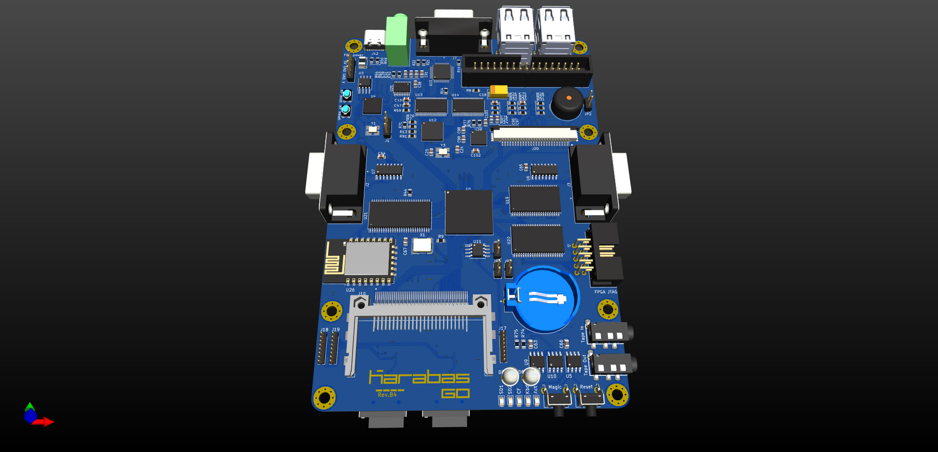
Main components on the Karabas go
Karabas go bill of materials (BOM)
279 components, 100 distinct parts — part numbers from the project's BOM.
| Qty | Part | Footprint | Refs |
|---|---|---|---|
| 1 | XC6SLX25-FTG256 | BGA-256_17.0x17.0mm_Layout16x16_P1.0mm_Ball0.5mm_Pad0.4mm_NSMD | U1 |
| 3 | LM1117MP-3.3 | SOT-223-3_TabPin2 | U2, U23, U27 |
| 2 | W25Q128JVSIQ W25Q128JVS | SOIC-8_5.23x5.23mm_P1.27mm | U3, U11 |
| 1 | RP2040 | RP2040-QFN-56 | U4 |
| 1 | PCA9536D | SOIC-8_3.9x4.9mm_P1.27mm | U5 |
| 2 | 74HC597 | SO-16_3.9x9.9mm_P1.27mm | U6, U7 |
| 1 | FE1.1S FE1.1s | SSOP-28_3.9x9.9mm_P0.635mm-long | U8 |
| 1 | 24LC08B | SO-8_3.9x4.9mm_P1.27mm | U9 |
| 1 | DS3231MZ | SOIC-8_3.9x4.9mm_P1.27mm | U10 |
| 1 | DS3231M | SOIC-16W_7.5x10.3mm_P1.27mm | U10'1 |
| 1 | FT812Q-T | QFN-56-1EP_8x8mm_P0.5mm_EP5.9x5.9mm_ThermalVias | U12 |
| 2 | MC74LCX16245DT | TSSOP-48_6.1x12.5mm_P0.5mm | U13, U14 |
| 1 | ADV7125BCPZ170 | QFN-48-1EP_7x7mm_P0.5mm_EP5.1x5.1mm_ThermalVias_plus_QFP-48 | U15 |
| 1 | 74LVC06 | SO-14_3.9x8.65mm_P1.27mm | U16 |
| 1 | 74LVC1G06 | SOT-23-5_HandSoldering | U17 |
| 1 | 74LVC14 | SO-14_3.9x8.65mm_P1.27mm | U18 |
| 2 | IS61WV20488BLL-10TLI | TSOP-II-44_10.16x18.41mm_P0.8mm | U19, U20 |
| 1 | MT48LC16M16A2TG | TSOP-II-54_22.2x10.16mm_P0.8mm | U21 |
| 1 | LM311 | SO-8_3.9x4.9mm_P1.27mm | U22 |
| 1 | LM1117MP-1.2 | SOT-223-3_TabPin2 | U24 |
Show 80 more
| Qty | Part | Footprint | Refs |
|---|---|---|---|
| 1 | PCM5102A | TSSOP-20_4.4x6.5mm_P0.65mm | U25 |
| 1 | ESP-12E | ESP-12E | U26 |
| 1 | SAM2695 | QFN-48-1EP_6x6mm_P0.4mm_EP4.66x4.66mm_BackHoles | U28 |
| 1 | MC4558 | SO-8_3.9x4.9mm_P1.27mm | U29 |
| 2 | BC856 | SOT-23 | Q1, Q3 |
| 1 | BC847 | SOT-23 | Q2 |
| 1 | 50 MHz | Oscillator_SMD_SeikoEpson_SG8002CA-4Pin_7.0x5.0mm | X1 |
| 2 | 12MHZ 12MHz | Crystal_SMD_3225-4Pin_3.2x2.5mm_HandSoldering | Y1, Y2 |
| 1 | 8MHZ 8MHz | Crystal_SMD_3225-4Pin_3.2x2.5mm_HandSoldering | Y3 |
| 1 | SWD | PinHeader_1x03_P2.54mm_Vertical | J1 |
| 2 | 2x USB A | USB_A_Wuerth_61400826021_Horizontal_Stacked_oval | J4, J5 |
| 1 | FPGA JTAG | IDC-Header_2x05_P2.54mm_Horizontal | J6 |
| 1 | FDD | IDC-Header_2x17_P2.54mm_Vertical | J8 |
| 2 | uSD card | Conn_uSDcard | J9, J11 |
| 1 | CF Card | TE_1734451-1-LONG | J10 |
| 1 | USB C | USB_C_Receptacle_XKB_U262-16XN-4BVC11 | J12 |
| 1 | Tape In | AUDIO_JACK_3.5MM_SMD_TRRS_rounded_mixed | J13 |
| 1 | Tape Out | AUDIO_JACK_3.5MM_SMD_TRRS_rounded_mixed | J14 |
| 1 | FDD power | PinHeader_1x04_P2.54mm_Vertical | J15 |
| 1 | Sound Out | Jack_3.5mm_CUI_SJ1-3535NG_Horizontal | J16 |
| 3 | EXT | PinHeader_1x08_P1.27mm_Vertical | J17, J18, J19 |
| 1 | FPC | TE_2-84952-6_1x26-1MP_P1.0mm_Horizontal | J20 |
| 1 | 3V | BAT_BS-7-BLUE | BT1 |
| 1 | RP Boot | SW_SPST_PTS810_handsoldering | BTN1 |
| 1 | RP Reset | SW_SPST_PTS810_handsoldering | BTN2 |
| 1 | 6V 2A | Fuse_1812_4532Metric_Pad1.30x3.40mm_HandSolder | F1 |
| 1 | Flash | PinHeader_1x02_P2.54mm_Vertical | JP1 |
| 1 | On/Off | PinHeader_1x02_P2.54mm_Vertical | JP2 |
| 1 | EXT CS (Beeper) | PinHeader_1x02_P2.54mm_Vertical | JP3 |
| 1 | EXT CS (Conf) | PinHeader_1x02_P2.54mm_Vertical | JP4 |
| 1 | Beeper | Buzzer_TDK_PS1240P02BT_D12.2mm_H6.5mm_long | LS1 |
| 1 | Magic | SW_Tactile_SPST_Angled_PTS645Vx58-2LFS | BTN3 |
| 1 | Reset | SW_Tactile_SPST_Angled_PTS645Vx58-2LFS | BTN4 |
| 1 | Keyboard | LED_0805_2012Metric_Pad1.15x1.40mm_HandSolder | D1 |
| 1 | Activitty | LED_0805_2012Metric_Pad1.15x1.40mm_HandSolder | D2 |
| 2 | LED_RAGB | LED_D5.0mm-4_RGB_tiny | D3, D8 |
| 1 | SD 2 | LED_0805_2012Metric_Pad1.15x1.40mm_HandSolder | D4 |
| 1 | CF | LED_0805_2012Metric_Pad1.15x1.40mm_HandSolder | D5 |
| 1 | 1N4148W | D_SOD-123 | D6 |
| 1 | SD 1 | LED_0805_2012Metric_Pad1.15x1.40mm_HandSolder | D7 |
| 4 | 10U 10u | C_0805_2012Metric_Pad1.18x1.45mm_HandSolder | C1, C7, C39, C43 |
| 3 | 1u | C_0805_2012Metric_Pad1.18x1.45mm_HandSolder | C2, C8, C28 |
| 2 | 22PF 22pF | C_0805_2012Metric_Pad1.18x1.45mm_HandSolder | C3, C4 |
| 64 | 100N 100n | C_0805_2012Metric_Pad1.18x1.45mm_HandSolder | C5, C6, C9, C10, C11, C12, C13, C14 +56 |
| 2 | 10UF 10uF | CP_EIA-7343-31_Kemet-D-uni | C18, C20 |
| 2 | 18PF 18pF | C_0805_2012Metric_Pad1.18x1.45mm_HandSolder | C23, C24 |
| 1 | 4U7 4u7 | CP_EIA-3216-18_Kemet-A_Pad1.58x1.35mm_HandSolder | C25 |
| 1 | 3N3 3n3 | C_0805_2012Metric_Pad1.18x1.45mm_HandSolder | C31 |
| 3 | 100UF 100uF | CP_EIA-7343-31_Kemet-D-uni | C37, C48, C49 |
| 1 | 2N2 2u2 | C_0805_2012Metric_Pad1.18x1.45mm_HandSolder | C38 |
| 2 | 2N2 2n2 | C_0805_2012Metric_Pad1.18x1.45mm_HandSolder | C42, C45 |
| 4 | 100N 100n | C_0603_1608Metric | C50, C51, C52, C53 |
| 3 | 4N7 4n7 | C_0805_2012Metric_Pad1.18x1.45mm_HandSolder | C88, C89, C90 |
| 2 | 470N 470n | C_0805_2012Metric_Pad1.18x1.45mm_HandSolder | C91, C92 |
| 8 | 100n | C_0805_2012Metric_Pad1.18x1.45mm_HandSolder | C95, C97, C99, C102, C103, C106, C107, C110 |
| 8 | 10u | C_0805_2012Metric_Pad1.18x1.45mm_HandSolder | C96, C98, C100, C101, C104, C105, C108, C109 |
| 17 | 1k | R_0805_2012Metric_Pad1.20x1.40mm_HandSolder | R1, R2, R7, R23, R24, R25, R26, R35 +9 |
| 17 | 10K 10k | R_0805_2012Metric_Pad1.20x1.40mm_HandSolder | R3, R4, R10, R11, R12, R13, R14, R39 +9 |
| 6 | 470 | R_0805_2012Metric_Pad1.20x1.40mm_HandSolder | R5, R6, R45, R46, R67, R69 |
| 1 | 2K7 2k7 | R_0805_2012Metric_Pad1.20x1.40mm_HandSolder | R8 |
| 3 | 27 | R_0805_2012Metric_Pad1.20x1.40mm_HandSolder | R9, R49, R50 |
| 5 | 75 | R_0805_2012Metric_Pad1.20x1.40mm_HandSolder | R15, R16, R17, R19, R20 |
| 1 | 0* | R_0805_2012Metric_Pad1.20x1.40mm_HandSolder | R18 |
| 9 | 22 | R_0805_2012Metric_Pad1.20x1.40mm_HandSolder | R21, R78, R79, R80, R81, R82, R83, R84 +1 |
| 1 | 510 | R_0805_2012Metric_Pad1.20x1.40mm_HandSolder | R22 |
| 6 | 330 | R_0805_2012Metric_Pad1.20x1.40mm_HandSolder | R27, R28, R29, R30, R31, R32 |
| 4 | 100 | R_0805_2012Metric_Pad1.20x1.40mm_HandSolder | R33, R34, R37, R38 |
| 1 | 1M | R_0805_2012Metric_Pad1.20x1.40mm_HandSolder | R47 |
| 3 | 5K1 5k1 | R_0805_2012Metric_Pad1.20x1.40mm_HandSolder | R48, R51, R53 |
| 1 | 33K 33k | R_0805_2012Metric_Pad1.20x1.40mm_HandSolder | R52 |
| 1 | 300 | R_0805_2012Metric_Pad1.20x1.40mm_HandSolder | R57 |
| 1 | 15k* | R_0805_2012Metric_Pad1.20x1.40mm_HandSolder | R58 |
| 2 | 470 10k | R_0805_2012Metric_Pad1.20x1.40mm_HandSolder | R63, R64 |
| 2 | 1k* | R_0805_2012Metric_Pad1.20x1.40mm_HandSolder | R72, R73 |
| 2 | 4K7 4k7 | R_0805_2012Metric_Pad1.20x1.40mm_HandSolder | R74, R75 |
| 2 | 4k7 | R_0805_2012Metric_Pad1.20x1.40mm_HandSolder | R76, R77 |
| 4 | 47k | R_0805_2012Metric_Pad1.20x1.40mm_HandSolder | R85, R89, R90, R91 |
| 1 | 27k | R_0805_2012Metric_Pad1.20x1.40mm_HandSolder | R86 |
| 2 | 3k3 | R_0805_2012Metric_Pad1.20x1.40mm_HandSolder | R87, R88 |
| 4 | 10K 10k | R_Array_Convex_4x0603 | RN1, RN2, RN3, RN4 |
Karabas go design files
The KiCad project lives in the andykarpov/karabas-go-pcb repository on GitHub; these links point at the commit this page was built from.
- Layoutkarabas-go.kicad_pcb
- Schematickarabas-go.kicad_sch
- BOMfab/karabas-go-bom.xlsx
Karabas go: common questions
What microcontroller does the Karabas go use?
The Karabas go is built around the RP2040, from the RP2040/RP2350 family.
How big is the Karabas go PCB?
The Karabas go measures 101.6 × 147.3 mm, has 4 copper layers and is 1.6 mm thick.
How many components are on the Karabas go?
279 components, from 100 distinct parts, with part numbers taken from the project's own BOM. The full bill of materials is listed on this page.
Where can I download the Karabas go design files?
From the andykarpov/karabas-go-pcb repository on GitHub, which has the KiCad layout, the schematic and the BOM; the links under Design files point to each one.
Can I use the Karabas go design in my own project?
It is published under CC-BY-NC-4.0, which limits how it may be reused; read the license before building on it.
Can I test firmware for the Karabas go without the hardware?
Yes. HardLabs builds a simulation of the board from its netlist and BOM, so you can run and debug RP2040/RP2350 firmware against it before you order a PCB.
More boards in karabas-go-pcb

Similar boards
 RP2040/RP2350
Open Book Abridged Edition
joeycastillo
85 × 115 mm29 parts2LCC-BY-SA-4.08.1k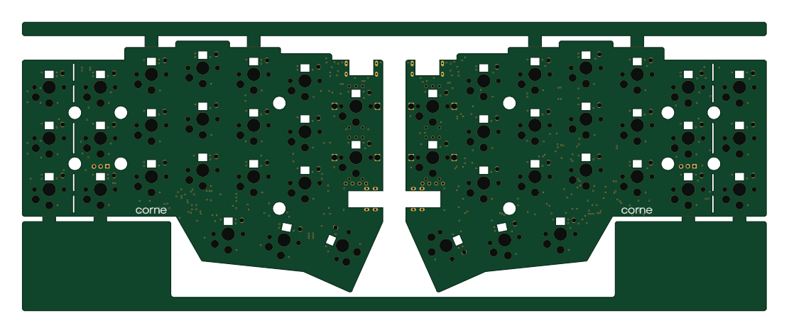 RP2040/RP2350
Corne
foostan
277.2 × 107.5 mm164 parts2LCC-BY-4.07.7k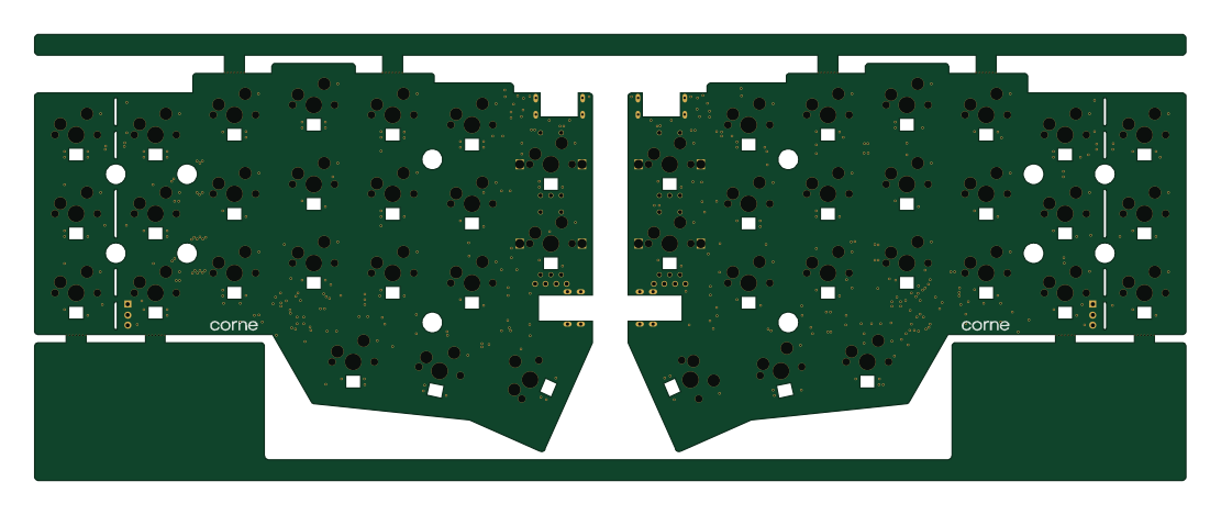 RP2040/RP2350
Corne
277.2 × 107.5 mm164 parts2LCC-BY-4.07.7k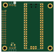 RP2040/RP2350
LogicAnalyzer
gusmanb
57 × 55.2 mm6 parts2LGPL-3.05.0k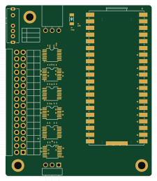 RP2040/RP2350
Jitx design
55.5 × 65 mm26 parts4LGPL-3.05.0k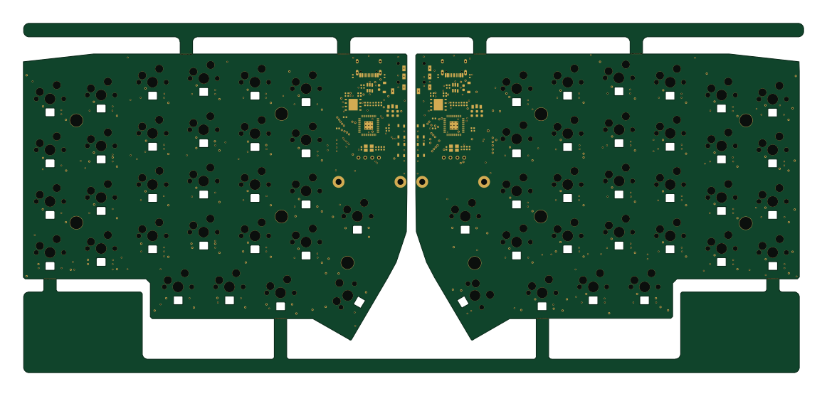 RP2040/RP2350
Pro V2
kata0510
290.1 × 130 mm270 parts2LMIT2.3k