
Eda designs

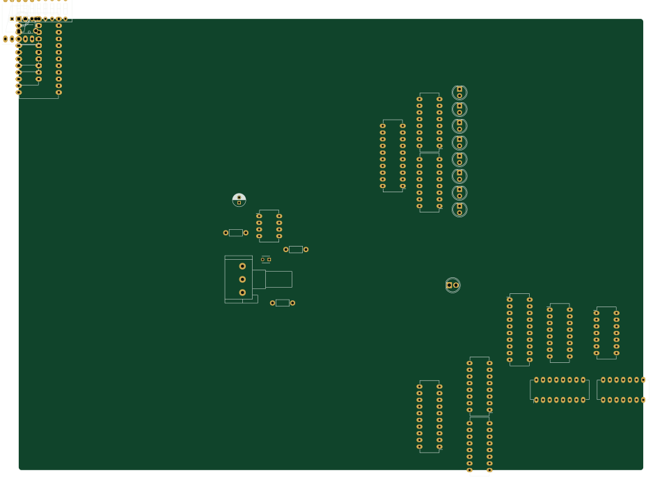
About the Eda designs PCB
Eda designs is an open source PCB design by kyllikki, published on GitHub under the MIT license. It is a 2-layer board measuring 237.5 × 171.5 mm, with 148 components from 41 distinct parts.
Other key parts include the 74LS86, 74LS283, 74LS245, NE555 and 74LS173. By type, the board carries 58 diodes, 44 ICs, 28 resistors, 8 capacitors, 6 switches and 4 LEDs.
From the project
EDA designs
Simple As Possible (SAP) computer by Ben Eater ==============================================
This is a schematic capture of this project derived from the excellent video series [1]
The design belongs to Ben, I just made a schematic in kicad
This schematic is released under CC BY-SA licence
[1] https://www.youtube.com/watch?v=HyznrdDSSGM&list=PLowKtXNTBypGqImE405J2565dvjafglHU
Main components on the Eda designs
Eda designs bill of materials (BOM)
148 components, 41 distinct parts.
| Qty | Part | Footprint | Refs |
|---|---|---|---|
| 2 | 74LS86 | DIP-16_W7.62mm_LongPads | U1, U2 |
| 1 | 74LS283 | DIP-20_W7.62mm_LongPads | U3 |
| 1 | 74LS283 | DIP-16_W7.62mm_LongPads | U4 |
| 2 | 74LS245 | DIP-16_W7.62mm_LongPads | U5, U9 |
| 1 | NE555 | DIP-20_W7.62mm_LongPads | U6 |
| 2 | 74LS173 | DIP-14_W7.62mm_LongPads | U7, U8 |
| 4 | 74LS173 | DIP-16_W7.62mm_LongPads | U10, U15, U16, U35 |
| 1 | 74LS173 | DIP-20_W7.62mm_LongPads | U11 |
| 1 | 74LS245 | DIP-8_W7.62mm_LongPads | U12 |
| 2 | 74LS161 | DIP-16_W7.62mm_LongPads | U13, U24 |
| 3 | 74LS245 | DIP-20_W7.62mm_LongPads | U14, U17, U43 |
| 2 | 74LS08 | DIP-14_W7.62mm_LongPads | U18, U33 |
| 3 | NE555 | DIP-8_W7.62mm_LongPads | U19, U30, U31 |
| 1 | 74LS273 | DIP-20_W7.62mm_LongPads | U20 |
| 1 | 74LS76 | DIP-16_W7.62mm_LongPads | U21 |
| 3 | 28C16 | DIP-24_W15.24mm_LongPads | U22, U25, U27 |
| 1 | 74LS139 | DIP-16_W7.62mm_LongPads | U23 |
| 1 | 74LS138 | DIP-16_W7.62mm_LongPads | U26 |
| 2 | 74HC04 | DIP-14_W7.62mm_LongPads | U28, U29 |
| 2 | 74LS04 | DIP-14_W7.62mm_LongPads | U32, U41 |
Show 21 more
| Qty | Part | Footprint | Refs |
|---|---|---|---|
| 1 | 74LS32 | DIP-14_W7.62mm_LongPads | U34 |
| 4 | 74LS157 | DIP-16_W7.62mm_LongPads | U36, U37, U40, U44 |
| 2 | 74LS189 | DIP-16_W7.62mm_LongPads | U38, U39 |
| 1 | 7400 | DIP-14_W7.62mm_LongPads | U42 |
| 2 | SW_SPDT | SW_Micro_SPST | SW1, SW4 |
| 2 | SW_Push | SW_PUSH_6mm_h9.5mm | SW2, SW6 |
| 1 | SW_DIP_x08 | SW_DIP_x8_Slide | SW3 |
| 1 | SW_DIP_x04 | SW_DIP_x4_Slide | SW5 |
| 4 | LTS-6980HR | 7SegmentLED_LTS6760_LTS6780 | AFF1, AFF2, AFF3, AFF4 |
| 58 | LED | LED-5MM | D1, D2, D3, D4, D5, D6, D7, D8 +50 |
| 1 | 0.1uF | C_Disc_D3_P2.5 | C1 |
| 1 | 1uF | C_Radial_D5_L11_P2 | C2 |
| 2 | 10n | C_Disc_D6_P5 | C3, C4 |
| 2 | 0.1uF | C_Disc_D6_P5 | C5, C6 |
| 2 | 0.1u | C_Disc_D6_P5 | C7, C8 |
| 7 | 1K | Resistor_Horizontal_RM7mm | R1, R4, R5, R22, R23, R24, R28 |
| 1 | 1M | Potentiometer_Alps-RK16-single | R2 |
| 3 | 220 | Resistor_Horizontal_RM7mm | R3, R26, R27 |
| 1 | 100K | Resistor_Horizontal_RM7mm | R6 |
| 15 | 470 | Resistor_Horizontal_RM7mm | R7, R8, R9, R10, R11, R12, R13, R14 +7 |
| 1 | 1M | Resistor_Horizontal_RM7mm | R25 |
Eda designs design files
The KiCad project lives in the kyllikki/eda-designs repository on GitHub; these links point at the commit this page was built from.
- LayoutSAP-BE/sap-be.kicad_pcb
Eda designs: common questions
How big is the Eda designs PCB?
The Eda designs measures 237.5 × 171.5 mm, has 2 copper layers and is 1.6 mm thick.
How many components are on the Eda designs?
148 components, from 41 distinct parts. The full bill of materials is listed on this page.
Where can I download the Eda designs design files?
From the kyllikki/eda-designs repository on GitHub, which has the KiCad layout; the links under Design files point to each one.
Can I use the Eda designs design in my own project?
Yes, under the terms of its MIT license, which kyllikki chose for the repository.