
1 open source board using the FLASH 2Mb
Real designs built with the FLASH 2Mb, from public GitHub projects: a quick way to see how others power, decouple and connect it. Each board comes with its KiCad files, full parts list and a render — and you can simulate its firmware on HardLabs.
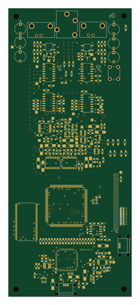
 smartbench
The FLASH 2Mb in open source designs
The gallery holds 1 open source boards using the FLASH 2Mb from 1 GitHub repository; a typical one measures about 67 × 157 mm and carries around 379 components.
100% use four copper layers or more, and 0% carry an open source license.
The most starred is ICE40hxk4 dev board by smartbench.
Microcontrollers on boards using the FLASH 2Mb
What boards using the FLASH 2Mb are built for
FLASH 2Mb: common questions
Where can I find a FLASH 2Mb reference design?
Each of the 1 boards on this page is a real design using the FLASH 2Mb. Open one to see how it is wired up, with the full BOM, a render of the layout and links to its KiCad files.
Which microcontrollers do boards using the FLASH 2Mb use?
Most are built on FPGA (1).
How big is a typical board using the FLASH 2Mb?
The median is 67 × 157 mm, and 0% are two-layer designs.
What is the most popular open source board using the FLASH 2Mb?
By GitHub stars, ICE40hxk4 dev board by smartbench, with 2 stars.
Can I simulate one of these boards using the FLASH 2Mb before building it?
Yes. HardLabs turns a board's netlist and BOM into a working simulation, so you can boot and test firmware against it with no hardware on your desk.