
3 open source boards using the TPS61176RTER
Real designs built with the TPS61176RTER, from public GitHub projects: a quick way to see how others power, decouple and connect it. Each board comes with its KiCad files, full parts list and a render — and you can simulate its firmware on HardLabs.
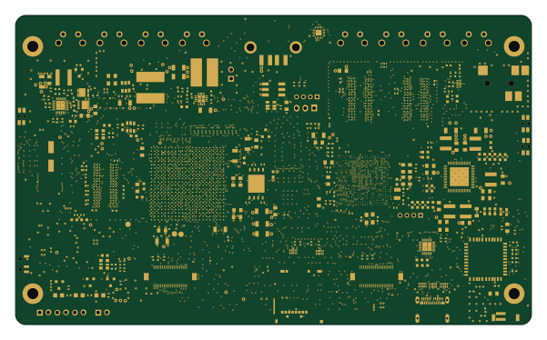 FPGA
FPGAMainboard
daveshah1
150 × 90 mm709 parts8LMIT40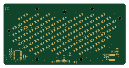
Lighthouse display
mwuerms
132 × 66.4 mm135 parts2LMIT0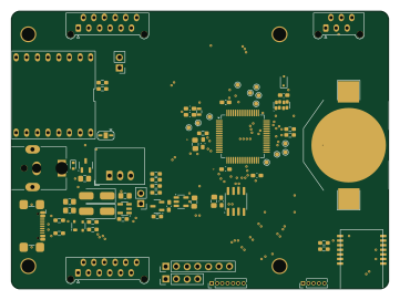 STM32
STM32Lighthouse Base
90 × 66.3 mm45 parts4LMIT0
The TPS61176RTER in open source designs
The gallery holds 3 open source boards using the TPS61176RTER from 2 GitHub repositories; a typical one measures about 132 × 66.4 mm and carries around 135 components.
67% use four copper layers or more, and 100% carry an open source license.
The most starred is Mainboard by daveshah1.
What boards using the TPS61176RTER are built for
TPS61176RTER: common questions
Where can I find a TPS61176RTER reference design?
Each of the 3 boards on this page is a real design using the TPS61176RTER. Open one to see how it is wired up, with the full BOM, a render of the layout and links to its KiCad files.
Which microcontrollers do boards using the TPS61176RTER use?
Most are built on FPGA (1) and STM32 (1).
How big is a typical board using the TPS61176RTER?
The median is 132 × 66.4 mm, and 33% are two-layer designs.
What is the most popular open source board using the TPS61176RTER?
By GitHub stars, Mainboard by daveshah1, with 40 stars.
Can I simulate one of these boards using the TPS61176RTER before building it?
Yes. HardLabs turns a board's netlist and BOM into a working simulation, so you can boot and test firmware against it with no hardware on your desk.