
Open source PCB designs you can simulate
7,464 boards
Every public KiCad project we can find on GitHub, with its processor, full parts list and a render of the board. Any of them can be brought up in simulation: open one and run firmware on it before you order a single PCB.
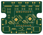 RP2040/RP2350
TundraIOExpansion
ras-marques
46 × 36.5 mm89 parts4LMIT29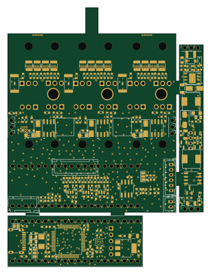 STM32
STM32FOC KING
b264
75.2 × 99.5 mm238 parts4LNo license3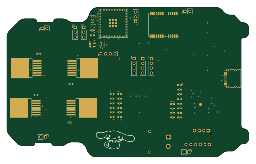 ESP32
ESP32Rc car
alaotach
129 × 79.8 mm85 parts4LNo license2
OpenBand
chancehowarth33
36 × 33.9 mm32 parts2LMIT1 Nordic nRF
Smartbag core
claudiofin
196 × 20 mm107 parts6LMIT0 Nordic nRF
Smartcube revA
manhoosbilli1
17.1 × 17.1 mm36 parts6LNo license0
BMI160-and-QMC5883L Second Bone
6.7 × 13.4 mm14 parts4LMIT29 Nordic nRF
Smartcube revA PCB A
17.1 × 17.1 mm28 parts6LNo license0
ICM-20948 First Bone
7 × 10.1 mm14 parts4LMIT29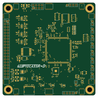 STM32
STM32AVIONICS BOARD
MatthiasGeorgImhof
80 × 80 mm178 parts4LCC-BY-NC-4.00
Smartcube revA CLEAN PCB A
15.5 × 15 mm27 parts6LNo license0
BMI270-and-QMC5883L
5 × 8.1 mm12 parts2LMIT29
BNO085 0x4A Board
8.1 × 8.8 mm12 parts4LMIT29
BNO085 0x4B Board
8.1 × 8.8 mm12 parts4LMIT29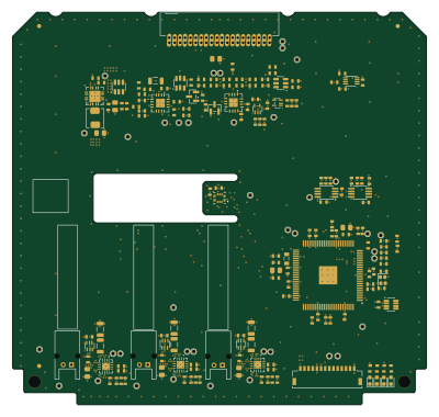
OreSat Mag Card
oresat
99.8 × 94.6 mm175 parts4LGPL-2.019
Multi imu
7.4 × 12.7 mm8 parts4LMIT29
ICM-20948 I2C 1V8 levels
4.4 × 6.6 mm7 parts4LMIT29
About these open source PCB designs
Every board here is a published hardware project: a public GitHub repository with KiCad design files and a bill of materials. HardLabs reads those files directly — the board outline for its size, the copper layers, every footprint for the parts list — and draws the render from the layout itself, so what you see is the design as committed rather than a product photo.
Boards are indexed by the microcontroller they are built around, by what they are for, and by every IC and module on them. That makes the gallery a quick way to find a reference design: look up a part number to see how other engineers power, decouple and connect it.
Using an open source board as a reference design
- Find boards built on your chip or with the part you are designing around.
- Compare their size, layer count and bill of materials, and open the KiCad files on GitHub.
- Check the license before reusing any of the design.
- Simulate the firmware on HardLabs to test your changes before you order a PCB.
Open source PCB designs: common questions
What is an open source PCB?
A printed circuit board whose design files — schematic, layout and bill of materials — are published for anyone to study and, depending on the license, to modify and manufacture.
Are these PCB designs free to use?
It depends on each project's license. Open hardware licenses such as CERN-OHL and CC BY-SA, and software licenses such as MIT, allow reuse on their terms; a repository with no license keeps all rights with its author. Every board page shows its license.
What design files do the boards come with?
They are KiCad projects: the .kicad_pcb layout and the schematic (or a netlist from older KiCad versions), plus a bill of materials, usually a CSV. Each board page links to those files in the original GitHub repository.
How do I find boards that use a specific part?
Search for the part number, or open the part's page from the list of parts. It shows every board built with that part and the parts most often used alongside it.
How many boards are there, and how often is the list updated?
7,464 boards from 3,597 repositories today. New projects are found and added every night.
Can I test a board's firmware before ordering the PCB?
Yes. HardLabs builds a simulation of a board from its netlist and BOM, so you can boot and debug firmware against it with no hardware on your desk.